Alphabetical Index
Browse by Elements
Keyword Search
Dry Etchants
Dry and Wet Etchants
Wet Etchants
Bulk Etchants
Layer Etchants
Nano Etchants
Single Crystal Etchants
Thin Film Etchants
Thin Foil Etchants
Wafer Etchants
Al Etchants
Cd Etchants
Ga Etchants
Ge Etchants
In Etchants
New Etchants
Other Etchants
Si Etchants
Zn Etchants
Help
Home
Tungsten Stringer Between Center Contacts
Material Name: Solder
Record No.: 182
Primary Chemical Element in Material: Cu
Sample Type: Wafer
Uses: No data
Etchant Name: None
Etching Method: No data
Etchant (Electrolyte) Composition: No data
Procedure (Condition): No data
Note: Figure 1 is photograph of a Tungsten
stringer defect discovered in failure analysis of a
minV(DD) outlier for a LSI Logic ASIC. The FA chip
was screened as an SPP outlier of the wafer’s intrinsic
minV(DD) distribution. This is an outlier from the
first step of the feed-forward minV(DD) test.
Reference: W. Robert Daasch, Parametric Variation or Defects?
Statistical Post-Processing Analysis of Wafer-Sort Data, ISTFA 2002, Proceedings of the 28th International Symposium for Testing and Failure Analysis, 3-7 November 2002, Phoenix Civic Center, Phoenix, Arizona, pp. 703-712.
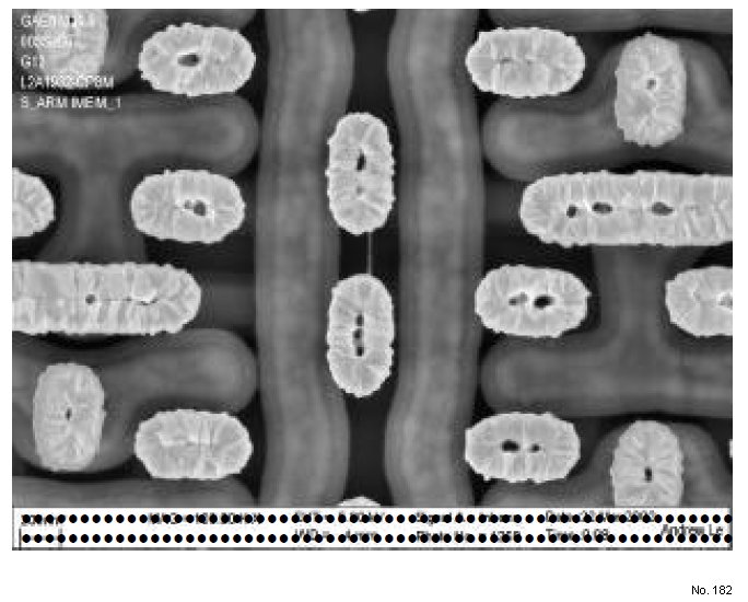
Figure 1: Failure Analysis of a minV(DD) outlier. Defect is the Tungsten stringer between center contacts.