Alphabetical Index
Browse by Elements
Keyword Search
Dry Etchants
Dry and Wet Etchants
Wet Etchants
Bulk Etchants
Layer Etchants
Nano Etchants
Single Crystal Etchants
Thin Film Etchants
Thin Foil Etchants
Wafer Etchants
Al Etchants
Cd Etchants
Ga Etchants
Ge Etchants
In Etchants
New Etchants
Other Etchants
Si Etchants
Zn Etchants
Help
Home
Gate Oxide Defects
Material Name: Silicon
Record No.: 184
Primary Chemical Element in Material: Si
Sample Type: Wafer
Uses: No data
Etchant Name: None
Etching Method: No data
Etchant (Electrolyte) Composition: No data
Procedure (Condition): No data
Note: Figure 6 shows the EBIC hot spots
at the upper left side of the image.
Combining a large viewing area and high
resolution, PTEM can be used for defect
searching and final observation. Figures 7, 8 and
9 show three PTEM images, each of them
addressing a different failure mechanism.
The first image reveals a particle on the silicon
substrate and the damage that particle caused.
The particle and the damaged area show different
contrast. Comparing this image with the XTEM
image in Figure 10, it can be seen that the PTEM
in this instance is better able to determine the
size and shape of the defect. The XTEM, on the
other hand, gives us a better perspective on its
exact position relative to the field oxide edge.
This type of defect is due to Kooi oxide, and is a
silicon-nitride residue on the silicon substrate.
The second PTEM image shows two gate oxide
pinholes. Keeping in mind that bright contrast in
the TEM means low atomic density, the bright
spot at the center of each pinhole indicates a
“hollow” core, and the dark ring indicates the
damaged substrate and poly. Examining the
image closely, in actuality we observe two
concentric rings. In the XTEM image we will
learn that one ring demonstrates the damaged
area in substrate and the other indicates the
damage are in poly. Again, the large area view of
the PTEM approach is useful for such multidefects
cases such as gate oxide damage
resulting from ESD events.
Figure 9 shows a crystal originated pit (COP).
These are imperfections in the silicon crystal,
and may result not only in yield but also
reliability failures, as the inferior quality gateoxide
locally breaks down over time.
The TEM fringe patterns can be interpreted as
thickness contours. In this image, the H-shaped
fringes delineate the active areas. A nodule like
defect can be seen at the edge of the gate. The
polysilicon gates and nitride spacer profiles can
also be observed as light “shadows” in the
image, while the high density tungsten plugs are
entirely opaque and thus readily discernible.
Although PTEM is great for searching and
finding the defect, localizing it on the silicon
plane, and measuring its total size and density,
Fab and R&D engineers typically prefer xsectional
views through the defect, which
provide precise layer and compositional
information. Figures 10, 11 and 12 are XTEM
images corresponding to each of the three defect
types discussed in figures 7, 8 and 9.
These images clearly demonstrate the layer that
defect is located in, and the damage it caused.
In Figure 10, the particle is on the silicon
substrate. Figure 11 shows the gate oxide
pinholes. The sample was parallel lapped and the
defect was located with EBIC (figures 5 and 6).
Because the sample has to be lapped down to the
poly layer to allow for a probe needle to touch it,
this sample has very thin poly layer. In this
image we can see the damage on silicon
substrate but not in poly.
With the XTEM approach in figure 13, the poly
was preserved, and the damage on both poly and
substrate can clearly be seen, corresponding to
the dark rings in the PTEM image.
Such a combination of an initial PTEM to
localize the defect, followed by an XTEM
through the defect, can be thought of as a type of
“three-dimensional” TEM, recently discussed in
the literature [10][11]. It solves the problem
having to guess at the defect position during
XTEM, but comes at a price – working with an
already very thin sample, which must now be
thinned along the other dimension.
The FIB has been used to prepare such samples
[9]. However, the beam damage that the FIB can
induce often results in poor TEM contrast.
Mechanical polishing of the PTEM sample to
form an XTEM sample solves this problem, but
requires exceptional skill. Figure 13 is such a
manually prepared sample.
The above results indicate three failure
mechanisms resulting in gate-oxide breakdown.
Each of them has distinct root cause. One is
residue-related and attributable to processing;
one is starting material related and attributable to
crystal defect (COPs); the last is test and
handling related and comes about as a result of
ESD damage. While traditional chemical
etching and decoration approaches would have
concluded “gate-oxide defect,” the underlying
real root cause would not have been clearly
identified, as it was using the above described
techniques.
Reference: Nathan Wang, Sabbas Daniel, TEM Direct Observation of Gate Oxide Defects, ISTFA 2002, Proceedings of the 28th International Symposium for Testing and Failure Analysis, 3-7 November 2002, Phoenix Civic Center, Phoenix, Arizona, pp. 765-769.
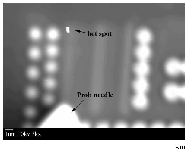
Figure 6: An EBIC image showing the hot spots
at end of poly line.

Figure 7: A PTEM image showing a residue in
the silicon substrate under the poly gate, causing
leakage current.
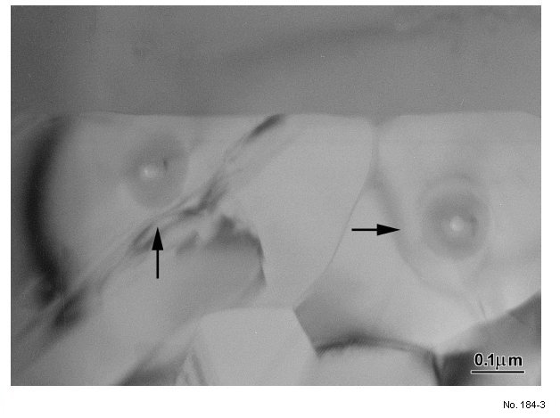
Figure 8: A PTEM image showing the gate oxide
pinholes on USB device.
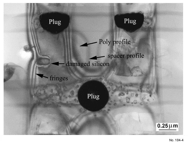
Figure 9: A PTEM image showing a crystal
originated pit in an SRAM device.

Figure 10: A XTEM image showing the bird’s
beak residue causing gate leakage.
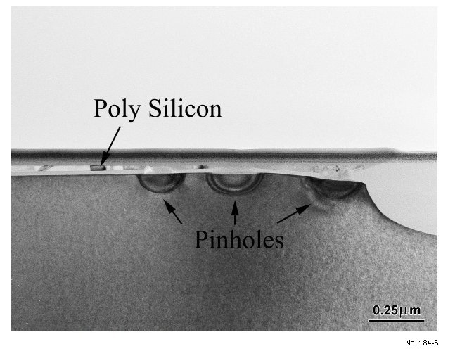
Figure 11: XTEM image showing the gate oxide
pinholes in the USB device.

Figure 12: XTEM image showing the crystal
originated pit in an SRAM device.
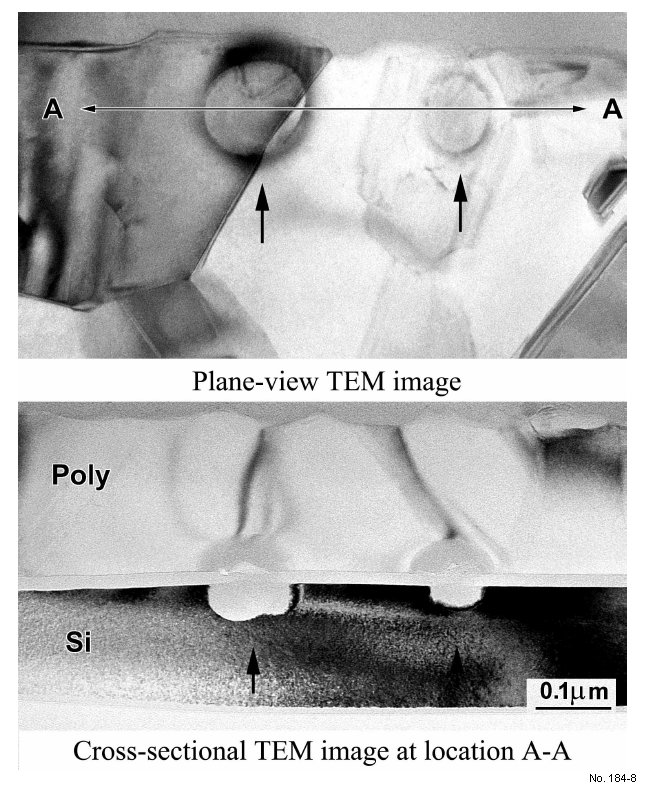
Figure 12: A three-dimensional TEM image
showing gate oxide pinhole.