Alphabetical Index
Browse by Elements
Keyword Search
Dry Etchants
Dry and Wet Etchants
Wet Etchants
Bulk Etchants
Layer Etchants
Nano Etchants
Single Crystal Etchants
Thin Film Etchants
Thin Foil Etchants
Wafer Etchants
Al Etchants
Cd Etchants
Ga Etchants
Ge Etchants
In Etchants
New Etchants
Other Etchants
Si Etchants
Zn Etchants
Help
Home
Solder Cracks
Material Name: Solder
Record No.: 187
Primary Chemical Element in Material: Cu
Sample Type: Bulk
Uses: Etching
Etchant Name: None
Etching Method: No data
Etchant (Electrolyte) Composition: No data
Procedure (Condition): No data
Note: No data
Reference: Sridhar Canumalla and Puligandla Viswanadham, Board Level Failure Mechanisms and Analysis in Hand-held Electronic
Products, Richard J. Ross (Editor), Microelectronics Failure Analysis, Desk Reference, Sixth Edition, ASM International, 2011, pp. 23-33.
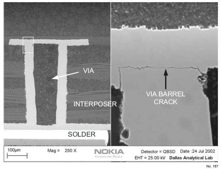
Figure 5: Via barrel cracking due to PWB level mechanical
loading causing electrical failure.

Figure 6: Crack in solder joint and ceramic component after
mechanical shock (drop) reliability testing.

Figure 7: Crack in solder joint after twist testing.

Figure 13: Interfacial fracture resembling brittle cleavage
between solder ball and pad.
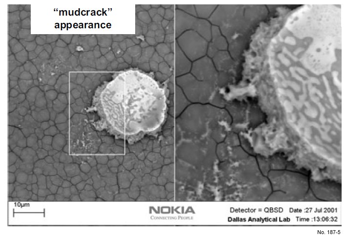
Figure 14: “Mud crack” appearance of Ni fracture surface
showing the poor bond quality of solder to Ni/Cu.

Figure 15: Hypercorrosion of Ni layer observed on a
microsectioned sample with black pad defect.

Figure 16: a) Build-up layer cracking in a solder joint with
trace and b) Optical micrograph (top view) of a sample
suspected to have a broken trace after the solder ball was
removed by mechanical polishing. The dotted line
represents the location and orientation of a second vertical
microsectioning needed to show damage under the pad.
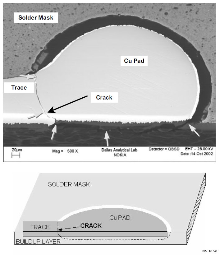
Figure 17: a) Trace fracture accompanied by build-up layer
cracking revealed in a double-cross sectioned sample
(sample shown different than that depicted in Figure 18), (b)
schematic showing the location of the crack in the build-up
layer.
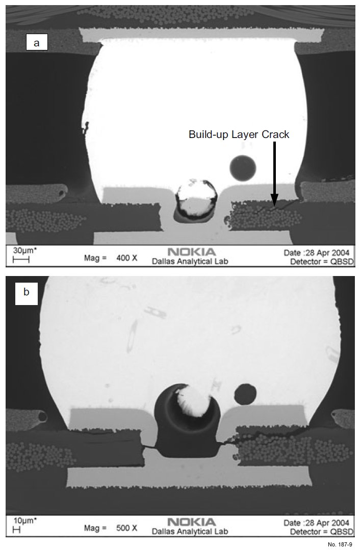
Figure 18: a) Build-up layer cracking in a solder joint with
via in pad b) further damage leading to via cracking upon
further exposure to mechanical drop related stresses.