Alphabetical Index
Browse by Elements
Keyword Search
Dry Etchants
Dry and Wet Etchants
Wet Etchants
Bulk Etchants
Layer Etchants
Nano Etchants
Single Crystal Etchants
Thin Film Etchants
Thin Foil Etchants
Wafer Etchants
Al Etchants
Cd Etchants
Ga Etchants
Ge Etchants
In Etchants
New Etchants
Other Etchants
Si Etchants
Zn Etchants
Help
Home
Tin Electrochemical Migration
Material Name: Sn
Record No.: 189
Primary Chemical Element in Material: Sn
Sample Type: Bulk
Uses: No data
Etchant Name: None
Etching Method: No data
Etchant (Electrolyte) Composition: No data
Procedure (Condition): No data
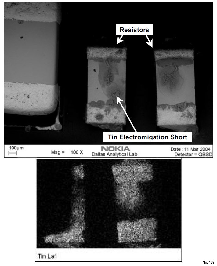
Note: Tin electrochemical migration mechanism is similar to that
of Cu, but is much more prevalent because Sn constitutes a
major portion of several commercial solder compositions
such as 62SnPb2Ag, 10SnPb, Sn3.5Ag0.7Cu, etc. In
addition, exposed Sn is more widespread on an assembled
PWB as compared to Cu. The particular example shown in
Figure 1 is from a test vehicle that failed upon exposure to
damp heat testing. In this case, the potential difference
between the terminals of a resistor with Sn termination
resulted in the migration of Sn from the cathode towards the
anode. It can be seen from the EDX elemental maps (Sn)
that one of the resistors is shorted.
Reference: Sridhar Canumalla and Puligandla Viswanadham, Board Level Failure Mechanisms and Analysis in Hand-held Electronic
Products, Richard J. Ross (Editor), Microelectronics Failure Analysis, Desk Reference, Sixth Edition, ASM International, 2011, pp. 23-33.

Figure 1: Tin electrochemical migration on a resistor with
pure tin termination.