Alphabetical Index
Browse by Elements
Keyword Search
Dry Etchants
Dry and Wet Etchants
Wet Etchants
Bulk Etchants
Layer Etchants
Nano Etchants
Single Crystal Etchants
Thin Film Etchants
Thin Foil Etchants
Wafer Etchants
Al Etchants
Cd Etchants
Ga Etchants
Ge Etchants
In Etchants
New Etchants
Other Etchants
Si Etchants
Zn Etchants
Help
Home
Process Induced Defects in Silicon Wafers
Material Name: Silicon
Record No.: 27
Primary Chemical Element in Material: Si
Sample Type: Wafer
Uses: Etching
Etchant Name: None
Etching Method: No data
Etchant (Electrolyte) Composition: No data
Procedure (Condition): No data
Note: Shown is a wafer that has been processed to some extent in order to produce integrated circuits. Four kinds of
defects were created that can be clearly distinguished, and (with some experience) identified as to their nature and
cause of generation.
The whole view of the wafer shows the polished front side (left) where not much is visible at this size. The backside
(right) has been intentionally roughened by a KOH etch, this accounts for the large scale structure (the intersecting
approximate rectangles) in the enlargements in the second half of the picture.
Reference: Website https://www.tf.uni-kiel.de/matwis/amat/elmat_en/index.html, 2020.
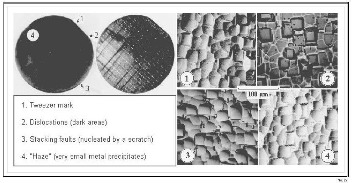
Figure 1: Process induced defects in silicon wafers.