Alphabetical Index
Browse by Elements
Keyword Search
Dry Etchants
Dry and Wet Etchants
Wet Etchants
Bulk Etchants
Layer Etchants
Nano Etchants
Single Crystal Etchants
Thin Film Etchants
Thin Foil Etchants
Wafer Etchants
Al Etchants
Cd Etchants
Ga Etchants
Ge Etchants
In Etchants
New Etchants
Other Etchants
Si Etchants
Zn Etchants
Help
Home
CMP-Induced Defects
Material Name: Copper
Record No.: 3
Primary Chemical Element in Material: Cu
Sample Type: Layer
Uses: Polishing
Etchant Name: None
Etching Method: Polishing
Etchant (Electrolyte) Composition: No data
Procedure (Condition): No data
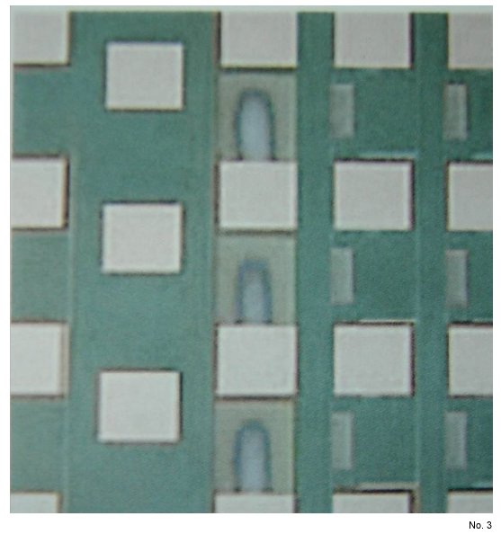
Note: CMP can reveal other defects – such as voids, seams, embedded particles,
incomplete patterning and other lithographic errors, random thickness variations, etc.
Reference: Arokia Nathan, Etching and Chemo-Mechanical Polishing, E&CE 493 Topic 2/730 Topic 13 – Nanoelectronics: Winter 2005, PowerPoint Presentation, pp. 1-35.

Figure 1: Lithographic errors and residual barrier pools.