Alphabetical Index
Browse by Elements
Keyword Search
Dry Etchants
Dry and Wet Etchants
Wet Etchants
Bulk Etchants
Layer Etchants
Nano Etchants
Single Crystal Etchants
Thin Film Etchants
Thin Foil Etchants
Wafer Etchants
Al Etchants
Cd Etchants
Ga Etchants
Ge Etchants
In Etchants
New Etchants
Other Etchants
Si Etchants
Zn Etchants
Help
Home
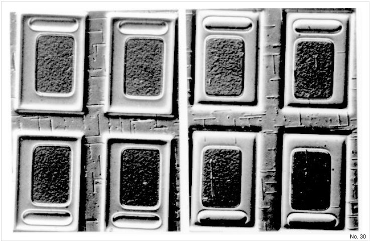
Defects in Transistors Revealed by Etching
Material Name: Silicon
Record No.: 30
Primary Chemical Element in Material: Si
Sample Type: Wafer
Uses: Etching
Etchant Name: None
Etching Method: No data
Etchant (Electrolyte) Composition: No data
Procedure (Condition): No data
Note: Stacking faults revealed by the so-called "Secco etch" for 30 seconds in transistors. For one kind of process we can
see different phases of the stacking fault generation by process-induced "forces" by looking at wafers from different
stages of the process.
Reference: Website https://www.tf.uni-kiel.de/matwis/amat/elmat_en/index.html, 2020.

Figure 1: Here we see bipolar transistors where just the collector contact (the oval part) and the base region (the rectangular
part) have been defined.