Alphabetical Index
Browse by Elements
Keyword Search
Dry Etchants
Dry and Wet Etchants
Wet Etchants
Bulk Etchants
Layer Etchants
Nano Etchants
Single Crystal Etchants
Thin Film Etchants
Thin Foil Etchants
Wafer Etchants
Al Etchants
Cd Etchants
Ga Etchants
Ge Etchants
In Etchants
New Etchants
Other Etchants
Si Etchants
Zn Etchants
Help
Home
Post Metal Etch Residue - Al Layer
Material Name: Aluminium
Record No.: 42
Primary Chemical Element in Material: Al
Sample Type: Layer
Uses: Etching
Etchant Name: None
Etching Method: Dry etching
Etchant (Electrolyte) Composition: No data
Procedure (Condition): No data
Note: After the TEOS hard mask was patterned, the remaining
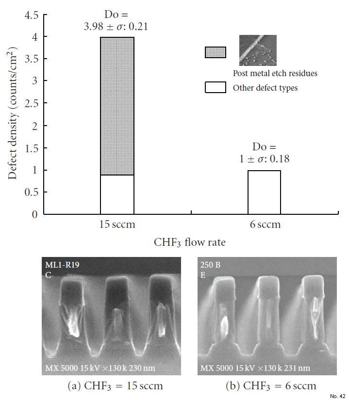
metal stack was etched on Alliance 9600PTX. Figure 5(a) shows the cross-sectional SEM micrograph of Al interconnect
etched using high CHF3 (15 sccm) flow rate during
the ME step in the starting etch baseline; the Al profile was
tapered and notch-free. Subsequently, the defect inspection
in die-to-die mode revealed the defect adder density around 3.98 defects/cm2 in average, in which the major defect type
is post metal etch residue (78% of total defect adders). Upon
SEM review, the residues are found to be concentrated near
the semi-iso Al-damaged sidewall and do not appear to be
randomly distributed. From the analysis of EDS spectrum
(see Figure 6) attained from a representative residue adder,
the defect contains Al, F, Cu, Si, and Cl atoms. The data
indicate that the residues are related to the attack of the
Al (0.5% Cu) sidewall by Cl atoms, and too much CHF3
addition in the ME step could passivate the surface of Al resulting in poor capability to remove the Al-containing
residues. As expected in Figure 5(b), the extent of Al residue
was decreased with decreasing CHF3 additive gas (6 sccm) in
the ME step; the ratio of Al residue to total defect adders was
suppressed from 78% to 2.7%. The reduction of the CHF3
flow rate in the ME step can effectively improve the post
metal etch residue issue, but it will also result in less passivant
on the metal sidewall to protect the Al bottom corner from
the attack of Cl atoms. As shown in Figure 5(b), a slight
bottom notching was observed on the Al corner. Therefore,
there is a tradeoff between Al notching elimination and
residue removal.
Reference: Hong-Ji Lee, Che-Lun Hung, Chia-Hao Leng, Nan-Tzu Lian, Ling-Wu Young,
Tahone Yang, Kuang-Chao Chen, and Chih-Yuan Lu, Etch Defect Characterization and Reduction in
Hard-Mask-Based Al Interconnect Etching, International Journal of Plasma Science and Engineering, Volume 2008, Article ID 154035, pp. 1-5.

Figure 1: (a) SEM micrograph of Al profile etched using 15 sccm of
CHF3 during the ME step. The major defect type is post metal etch
residue (78% of total defect adders). (b) The ratio of post metal etch
residue to total defect adders was decreased to 2.7% at the lower
CHF3 flow of 6 sccm; however, there is a slight Al bottom notching
observed from physical profile.Defect density (Do) was expressed as
means ± standard deviation (sigma) in counts/cm2. Each etch condition
was tested on three wafers.