Alphabetical Index
Browse by Elements
Keyword Search
Dry Etchants
Dry and Wet Etchants
Wet Etchants
Bulk Etchants
Layer Etchants
Nano Etchants
Single Crystal Etchants
Thin Film Etchants
Thin Foil Etchants
Wafer Etchants
Al Etchants
Cd Etchants
Ga Etchants
Ge Etchants
In Etchants
New Etchants
Other Etchants
Si Etchants
Zn Etchants
Help
Home
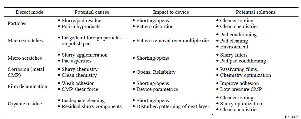
Potential Causes of CMP Defects and possible Solutions
Material Name: No data
Record No.: 44
Primary Chemical Element in Material: No data
Sample Type: Wafer
Uses: Polishing
Etchant Name: None
Etching Method: Polishing
Etchant (Electrolyte) Composition: No data
Procedure (Condition): No data
Note: In the manufacturing of IC chips, the wafer is polished
several times using the CMP process. CMP has been
applied for polishing various types of surfaces,
including oxides, Cu, W and others. However,
several defects induced by CMP depend on the type of surface being polished. This may be attributed to
the effects of various chemicals and abrasive particles
as well as the pressure exerted on the wafer surface. Defects typically formed during the CMP
process include organic residues, water marks,
particle adherence and impingement, corrosion
pit, and scratches. However, the removal of
organic residues and water mark formation are trivial
in oxide CMP, but other types of defects, such as
scratch formation, are critical, as they affect the yield
and reliability of the devices. Table 1 shows the
CMP process induced defects and their specific effects
on the replacement metal gate (RMG) process.
Scratches are one of the most commonly generated
defects during the CMP process. It was found that CMP
scratches could cause an initial failure as well as long
term reliability failure. The failure mechanism in
the shallow trench isolation (STI), inter-level dielectric
(ILD), and poly-Si CMP processes is very similar in
nature. Scratches cannot be detected after CMP, but are
usually identified after etching using the HF solution. The periodic arc scars generated on brittle
materials such as oxide, BPSG, and poly-Si are called
chatter mark-type scratches. Figure 1 shows
some examples of chatter mark scratches after STI
CMP. Scratch shape is influenced by the mechanical
properties of the material. A wide variety of scratches
are formed on a metal surface like Cu, which is
shown in Fig. 2.
Reference: Tae-Young KWON, Manivannan RAMACHANDRAN, Jin-Goo PARK, Scratch formation and its mechanism in chemical mechanical
planarization (CMP), Friction 1(4): 279–305 (2013).
Table 1: Potential causes of CMP defects and possible solutions.


Figure 1: Chatter mark scratches observed in STI CMP.

Figure 2: Various scratches formed in Cu CMP.