Alphabetical Index
Browse by Elements
Keyword Search
Dry Etchants
Dry and Wet Etchants
Wet Etchants
Bulk Etchants
Layer Etchants
Nano Etchants
Single Crystal Etchants
Thin Film Etchants
Thin Foil Etchants
Wafer Etchants
Al Etchants
Cd Etchants
Ga Etchants
Ge Etchants
In Etchants
New Etchants
Other Etchants
Si Etchants
Zn Etchants
Help
Home
Scratch Level on STI Patterned Wafers
Material Name: No data
Record No.: 48
Primary Chemical Element in Material: No data
Sample Type: Wafer
Uses: Polishing
Etchant Name: None
Etching Method: Polishing
Etchant (Electrolyte) Composition: No data
Procedure (Condition): No data
Note: During the CMP process, the pad surface can
undergo plastic deformation and the surface becomes
smoother as the pores are filled with the pad materials. Using a glazed pad causes the removal rate to
drop significantly. Polishing pads were conditioned
with a diamond conditioner to provide consistent
performance and to prevent the glazing effect. Usually,
diamond grits used for pad conditioning are attached
to an alloy substrate using electrochemical deposition
methods. Yang et al. investigated the CMP
process based on material removal rate and scratch
defects by studying the pad interaction and conditioner
effect using two types of polishing pads: a porous
pad and a solid pad with micro holes (Fig. 24). When
a solid pad with micro holes was used with a fumed
silica slurry and a 180 µm diamond grit conditioner,
the material removal rate decreased by approximately
10% compared with the porous pad. However, the
scratch defects were reduced when compared with
the porous pad which is shown in Fig. 25. In order to
increase the removal rate obtained using a solid pad
with micro holes to a level comparable to a regular
porous pad, various diamond conditioners with
diamond size ranging from 70 to 130 µm were adopted.
Also, pad surface roughness and contact area were
analyzed to understand the removal rate and the
scratch generation. Figure 26 shows the effect of diamond size of conditioner on the removal rate and
scratch generation. It was found that the micro holes
in the pad acted as a defect source or coarse particle
reservoir to prevent micro scratching during the
process. They reported optimized results of solid
pads with micro holes using the hole depth control
procedure to reduce the defects.
As mentioned earlier, pad debris can be generated
due to tearing of the pad by the conditioner. Prasad
et al. studied the generation of pad debris and its
characterization. They reported that pad debris could
act as a main scratch source, resulting in scratches with
several size ranges with irregular shapes, mostly in
agglomerated form. It was also proposed that the
surface properties were changed by their adsorption with abrasive particles. Figure 27 shows FESEM images
of fresh pad particles and pad debris generated using
DI water and silica abrasive particles. Park’s group also investigated the scratch number using the
three different scratch source (vis., pad debris, dried
particles, and diamond particles) on scratch formation
comprehensively with their classification. Figure 28
shows the material removal rate and generated scratch
number as a function of scratch source. A small
amount of impurity in slurry did not affect the MRR.
However, scratch number was affected by the kind of
scratch sources. Figure 29 shows the distribution of
scratchess formed by adding different scratch sources
during polishing. Borken chatter type of scratches
was easily formed when dry slurry paritcles were
added but group chatter when pad debris were added.
Yang et al. measured the pad surface hardening phenomenon based on force–distance (F–D) curves.
It was found that the interaction between abrasive
particle and polyurethane pad under tribo-mechanical
action could change the pad surface hardness. Benner
et al. used a vacuum cleaner to remove the pad
debris and agglomerated large particles from the pad;
they dubbed this process the pad surface manager
(PSM). Figure 30 contains a plot of light-point defects
measured using a Tencor 6220 on polished oxide
wafers using different levels of PSM vacuum. The data
were normalized to that observed without vacuum.
As the PSM vacuum level was increased, CMP
induced wafer defects decreased. Approximately a
50% reduction in light-point defects was observed
using the PSM technique.
Reference: Tae-Young KWON, Manivannan RAMACHANDRAN, Jin-Goo PARK, Scratch formation and its mechanism in chemical mechanical
planarization (CMP), Friction 1(4): 279–305 (2013).
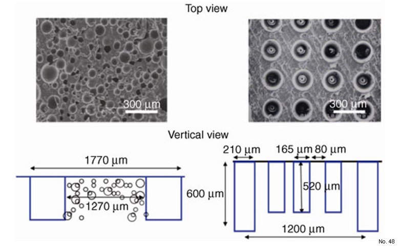
Figure 24: SEM micrographs (top) and schematics (bottom) of (a)
porous pads and (b) solid pads.
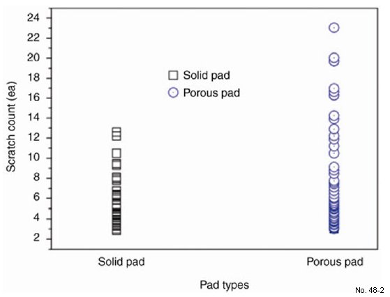
Figure 25: Scratch level on STI patterned wafers generated by porous
and solid pads with 180 µm diamond conditioner.

Figure 26: The effect of diamond size on (a) removal rate and (b)
scratch generation.

Figure 27: SEM image and EDX analysis of (a) fresh pad, (b) pad
debris with only DI water, and (c) pad debris with silica slurry.
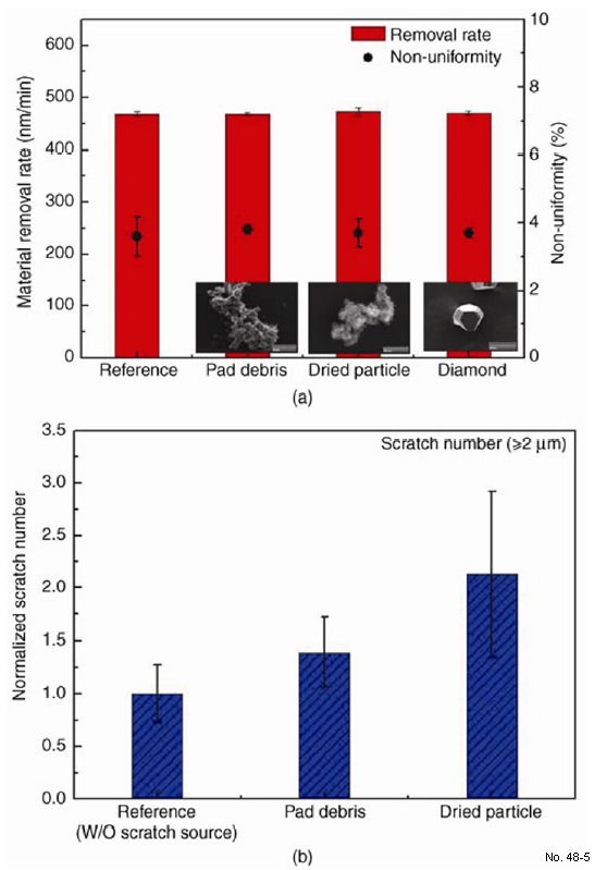
Figure 28: (a) Material removal rate, non-uniformity and (b) the
variation of number of scratches formed with addition of different
scratch sources.
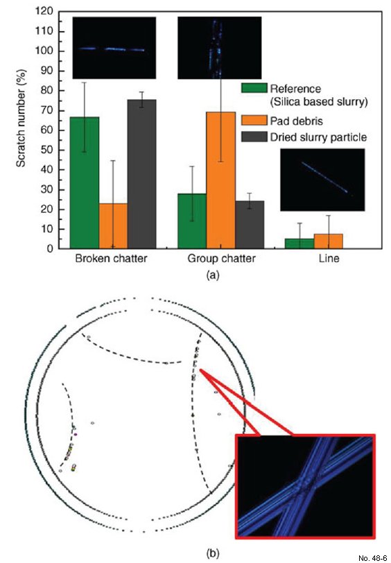
Figure 29: (a) Effect of addition of pad debris, dried slurry particle
and (b) diamond particles on distribution of scratch shapes formed
on oxide surface after CMP process with silica slurry.

Figure 30: A plot of the dependence of light-point defect counts,
measured with a Tencor 6220 on oxide wafers, as a function of
PSM vacuum level. A reduction of nearly 50% was observed as a
PSM vacuum.