Alphabetical Index
Browse by Elements
Keyword Search
Dry Etchants
Dry and Wet Etchants
Wet Etchants
Bulk Etchants
Layer Etchants
Nano Etchants
Single Crystal Etchants
Thin Film Etchants
Thin Foil Etchants
Wafer Etchants
Al Etchants
Cd Etchants
Ga Etchants
Ge Etchants
In Etchants
New Etchants
Other Etchants
Si Etchants
Zn Etchants
Help
Home
Chatter Surface Damage
Material Name: No data
Record No.: 51
Primary Chemical Element in Material: No data
Sample Type: Wafer
Uses: Polishing
Etchant Name: None
Etching Method: Polishing
Etchant (Electrolyte) Composition: No data
Procedure (Condition): No data
Note: Typically, chatter mark-type scratches, which have
a repetitive C-shaped crack, were generated in interlevel
dielectric (ILD) materials (Fig. 1). In this image,
the cracks are larger at one end and smaller at the other
end of the repetitive line. Furthermore, the repetitive
C-shaped surface showed damage that is tens of nm
deep with some individual cracks that were deeper
than others, in atomic force microscope (AFM) images.
Ring et al. explained this phenomenon based on
bouncing particle model. The springiness of the pad
causes the particle to bounce against the wafer surface.
Bouncing may be initiated by a particle impurity that
is sliding across the surface of the wafer. After the first
bounce, the particles have sufficient force to indent
the surface of the wafer. This force is supplied by
the elastic properties of the pad when the particle is
pushed into it and then rebounds. The frequency of
bounces can be determined by the simple physics of a
mass (the particle) on a spring (the pad).
Reference: Tae-Young KWON, Manivannan RAMACHANDRAN, Jin-Goo PARK, Scratch formation and its mechanism in chemical mechanical
planarization (CMP), Friction 1(4): 279–305 (2013).
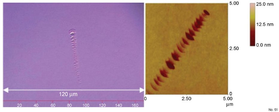
Figure 1: Chatter surface damage showing repetitive, 40-nm-deep indentations in the wafer surface.