Alphabetical Index
Browse by Elements
Keyword Search
Dry Etchants
Dry and Wet Etchants
Wet Etchants
Bulk Etchants
Layer Etchants
Nano Etchants
Single Crystal Etchants
Thin Film Etchants
Thin Foil Etchants
Wafer Etchants
Al Etchants
Cd Etchants
Ga Etchants
Ge Etchants
In Etchants
New Etchants
Other Etchants
Si Etchants
Zn Etchants
Help
Home
Hollows, Hillocks - Copper Wafer
Material Name: Copper
Record No.: 53
Primary Chemical Element in Material: Cu
Sample Type: Wafer
Uses: Cleaning
Etchant Name: None
Etching Method: Cleaning
Etchant (Electrolyte) Composition: No data
Procedure (Condition): No data
Note: To develop a more reliable plasma cleaning process, the H2 /N2
mixture plasma is suggested for Cu dual damascene process. First,
the Cu wafer was exposed to N2 plasma with the SWP source.
Compared with the control sample, the Cu surface showed no obvious
change as observed by the SEM technique. However, when the
Cu wafer was exposed to H2 plasma at 250°C, many holes formed
on the Cu surface, as shown in Fig. 5. For the control sample, native
Cu oxides were formed on the surface when the Cu wafer was
exposed to air.
When the Cu wafer was exposed to H2 /N2 (3.75-7.5%) plasma with the SWP source at 250°C, hillocks
formed obviously on the Cu surface, as shown in Fig. 8. Seen in Fig.
9, the top view of the sample undergoing longer plasma cleaning
inspected by the SEM technique reveals the formation of hillocks
and cracks along the grain boundary. The mechanism of this hillock
formation merits further investigation.
The Cu wafer was transferred from the left load-lock chamber
(wafer chuck was set at 80°C) to the reaction chamber for 5-10 min
(the wafer chuck was set at 250-350°C), and then transferred back. In the reaction chamber, when pure
H2 or pure N2 or H2 /N2 mixed gases was used without plasma
cleaning, no obvious hillocks were formed on the Cu surface, even
when the temperature of the chuck was increased up to 350°C. Some
research has reported that metal ~example, aluminum! has a higher
coefficient of thermal expansion than silicon or silicon dioxide.
When metal films on the silicon substrate or silicon oxide are heated
(for example to 450°C sintering) during device manufacturing process,
they undergo compressive stress, which can be relieved by
hillock formation. On the contrary, when metal films on silicon substrate
or silicon oxide are cooled during the device manufacturing
process, they undergo tensile stress, which results in crack formation.
However, no obvious change on the Cu surface was observed
by the SEM technique, compared with the control sample. The experimental
results mentioned above revealed that thermal stress
from the chuck temperature is not the dominant mechanism for Cu
hillock formation. In this case, the range of chuck temperature variation
from 80 to 350°C was the largest. It is believed that the range of
temperature variation was still too small to form Cu hillocks or
cracks. According to the data mentioned above, hillocks occur on the Cu surface mainly after plasma cleaning. Therefore, it is believed
that plasma cleaning plays a dominant role in hillock formation.
Previous studies have reported that aluminum hillock growth is
enhanced during the early stage of insulator deposition. The enhanced
formation of hillocks is attributed to the increase in substrate
temperature with the application of radio frequency (rf) power.
Reference: Tsung-Kuei Kang, and Wei-Yang Chou, Avoiding Cu Hillocks during the Plasma Process, Journal of The Electrochemical Society, 151 (6) G391-G395, 2004.
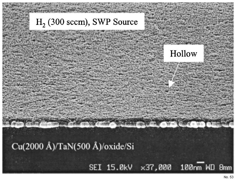
Figure 5: SEM micrograph of Cu sample plasma-induced by pure H2
plasma (SWP source).
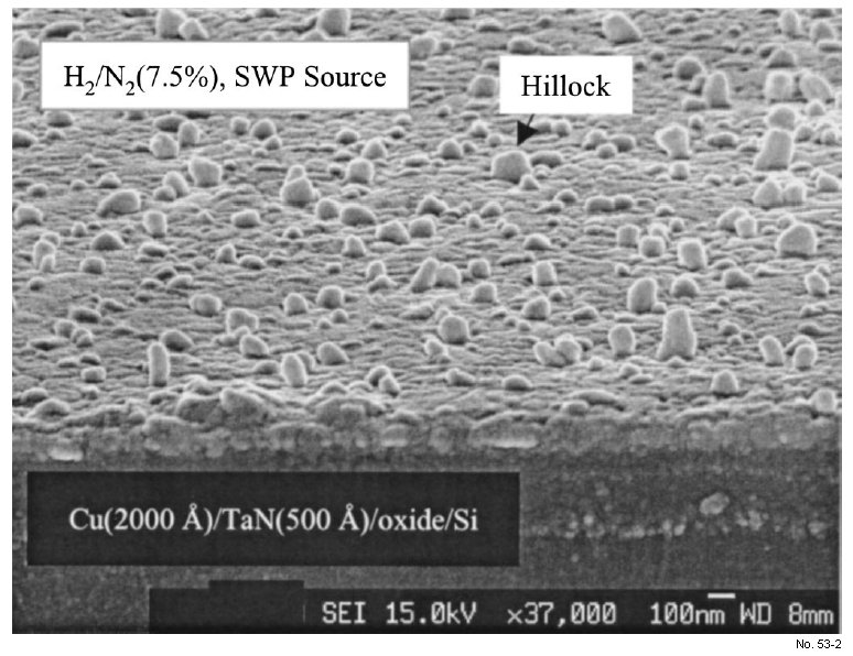
Figure 8: SEM micrograph of Cu sample plasma-induced by H2 /N2 plasma
(SWP source).

Figure 9: Top-view SEM micrograph of Cu sample plasma-induced by
H2 /N2 plasma for a long time (SWP source).