Alphabetical Index
Browse by Elements
Keyword Search
Dry Etchants
Dry and Wet Etchants
Wet Etchants
Bulk Etchants
Layer Etchants
Nano Etchants
Single Crystal Etchants
Thin Film Etchants
Thin Foil Etchants
Wafer Etchants
Al Etchants
Cd Etchants
Ga Etchants
Ge Etchants
In Etchants
New Etchants
Other Etchants
Si Etchants
Zn Etchants
Help
Home
Example of an Unsuccessful Cr Lift Off
Material Name: Silicon
Record No.: 56
Primary Chemical Element in Material: Wafer
Sample Type: Layer
Uses: Etching
Etchant Name: None
Etching Method: Dry etching
Etchant (Electrolyte) Composition: No data
Procedure (Condition): No data
Note: There were also unsatisfactory results when using the Cr
lift-off process instead of the Cr wet etch. This was because
of a thin metal film on top of the photoresist, which came
into contact with the metal layer during deposition. This
caused a ripping effect during lift-off, as shown in Fig. 9 and
explained schematically in Fig. 10. This effect resulted in a
rough edge on the metal hard mask in Fig. 9 (the holes
shown in this figure were from an early mask design with
0.5-mm-diameter holes). These rough edges created undesirable
distortions in the hole profiles.
Reference: Ankita Verma, Joshah Jennings, Ryan D. Johnson, Marc H. Weber, and Kelvin G. Lynn, Fabrication of 3D charged particle trap using through-silicon vias etched by
deep reactive ion etching, J. Vac. Sci. Technol. B 31, 032001 (2013); doi: 10.1116/1.4799662.
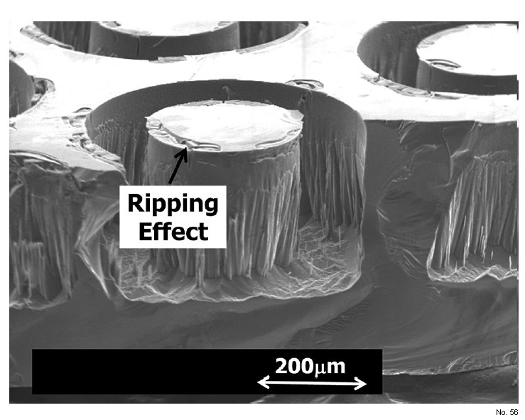
Figure 9: Example of an unsuccessful Cr lift off.