Alphabetical Index
Browse by Elements
Keyword Search
Dry Etchants
Dry and Wet Etchants
Wet Etchants
Bulk Etchants
Layer Etchants
Nano Etchants
Single Crystal Etchants
Thin Film Etchants
Thin Foil Etchants
Wafer Etchants
Al Etchants
Cd Etchants
Ga Etchants
Ge Etchants
In Etchants
New Etchants
Other Etchants
Si Etchants
Zn Etchants
Help
Home
Example of Notching and Bowing Occuring in an Etched Sample
Material Name: Silicon
Record No.: 59
Primary Chemical Element in Material: Wafer
Sample Type: Wafer
Uses: Etching
Etchant Name: None
Etching Method: Dry etching
Etchant (Electrolyte) Composition: No data
Procedure (Condition): No data
Note: Notching/footing: Notching and footing occur at the bottom of the etched
hole and the ions affect the oxide at the wafer back. The oxide
is a nonconducting material that accumulates negative charges
on its surface and leads to the deflection of the positive ions in
the plasma. These deflected ions start etching into the Si walls
at the bottom of the hole, as shown in Fig. 1. It may be possible
to prevent notching by using a conducting material at the
bottom of the wafer, so that the conducting material will not
accumulate a charge and deflect the ions. To test this hypothesis,
aluminum (Al) was deposited on the back side of a wafer
as an etch stop, but the Al layer, being only 0.0005 mm thick,
started breaking away faster than the oxide. Also, the thermal
conduction was better on the Al etching surface than on the
oxide, which changed the hole profile. The crystallographic
effect appeared at the bottom of the holes. If the Al backing
remained, the table temperature would need to be increased
by at least 10 .C to stop the crystallographic angles (which are
explained later in this section) forming at the hole bottom.
Reference: Ankita Verma, Joshah Jennings, Ryan D. Johnson, Marc H. Weber, and Kelvin G. Lynn, Fabrication of 3D charged particle trap using through-silicon vias etched by
deep reactive ion etching, J. Vac. Sci. Technol. B 31, 032001 (2013); doi: 10.1116/1.4799662.
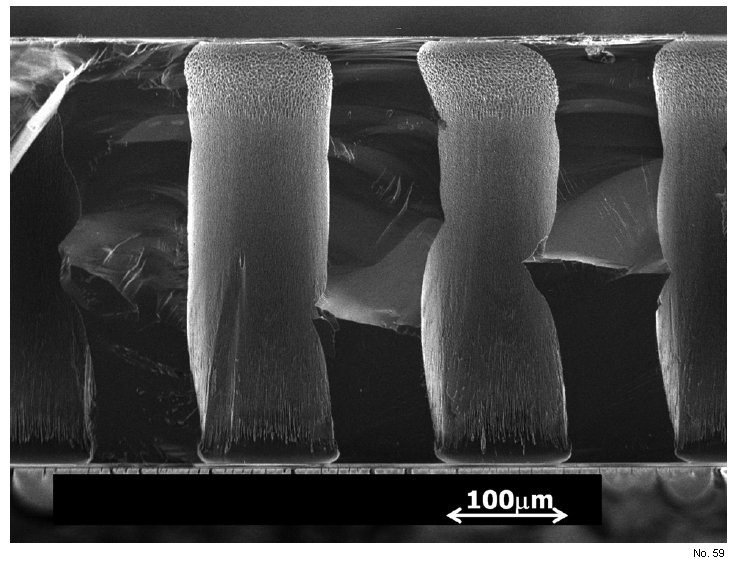
Figure 1: Example of notching and bowing occuring in an etched sample.