Alphabetical Index
Browse by Elements
Keyword Search
Dry Etchants
Dry and Wet Etchants
Wet Etchants
Bulk Etchants
Layer Etchants
Nano Etchants
Single Crystal Etchants
Thin Film Etchants
Thin Foil Etchants
Wafer Etchants
Al Etchants
Cd Etchants
Ga Etchants
Ge Etchants
In Etchants
New Etchants
Other Etchants
Si Etchants
Zn Etchants
Help
Home
Sidewall Damage - Silicon - Dry Etching
Material Name: Silicon
Record No.: 60
Primary Chemical Element in Material: Si
Sample Type: Wafer
Uses: Etching
Etchant Name: None
Etching Method: Dry etching
Etchant (Electrolyte) Composition: No data
Procedure (Condition): No data
Note: In Figure 1, some obvious sidewall
damage can be seen in the trenches etched at a bias
power of 35W. As the bias power increases, the uniformity
of the ions decreases. This is caused by the fact
that some plasmas bombard the sidewall before reaching
the bottom during the etching cycle. On the upper
side of the trench’s sidewall, the polymer materials of
the deposition layer, along with some silicon, are partly
removed by the bombardment of the ions, which leads
to a rapid expansion of the trench’s width. On the
lower parts of the sidewall, the sputtered polymer materials
will redeposit onto the sidewall and form new
deposition layers, which makes it thicker than the
layers on the upper sidewalls. Several intense redeposition
functions generated by high bias power may again
shrink the width of the lower parts of the trenches,
which also facilitates sidewall damage.
Reference: Tiantong Xu, et al., Effects of deep reactive ion etching
parameters on etching rate and surface morphology in extremely deep silicon etch process with high aspect ratio, Advances in Mechanical Engineering, 2017, Vol. 9(12) 1–19, DOI: 10.1177/1687814017738152.
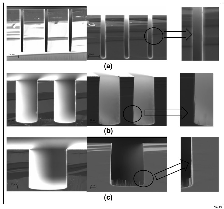
Figure 1: (a) SEM cross section of 6-mm-wide trenches, etched by bias power levels of 15 and 35 W, respectively. Sidewall damage
can be seen in the 35 W trenches. (b) SEM cross section of 55-mm-wide trenches, etched by bias power levels of 15 and 35 W,
respectively. Sidewall damage can be seen in the 35 W trenches. (c) SEM cross section of 110-mm-wide trenches, etched by bias
power levels of 15 and 35 W, respectively. Sidewall damage can be seen in the 35 W trenches.