Alphabetical Index
Browse by Elements
Keyword Search
Dry Etchants
Dry and Wet Etchants
Wet Etchants
Bulk Etchants
Layer Etchants
Nano Etchants
Single Crystal Etchants
Thin Film Etchants
Thin Foil Etchants
Wafer Etchants
Al Etchants
Cd Etchants
Ga Etchants
Ge Etchants
In Etchants
New Etchants
Other Etchants
Si Etchants
Zn Etchants
Help
Home
Blocked Etch Macro Defect
Material Name: Wafer
Record No.: 63
Primary Chemical Element in Material: No data
Sample Type: Wafer
Uses: Etching
Etchant Name: None
Etching Method: Etching
Etchant (Electrolyte) Composition: No data
Procedure (Condition): No data
Note: Blocked Etch defects are typically due to clamp-ring polymer delamination from plasma etch tools. These semiconductor wafer defects are caused by polymer build up on the etcher clamp ring that relocates laminate materials into the wafer placement area. Etch is blocked by a layer of detached polymer film. You can see in some examples above, the semiconductor wafer defect may appear to be identical and affect multiple wafers in a lot or even multiple lots.
Reference: Website https://www.microtronic.com/defect-library/blocked-etch-macro-defect/, Image and text by courtesy of Microtronic company, 2020.
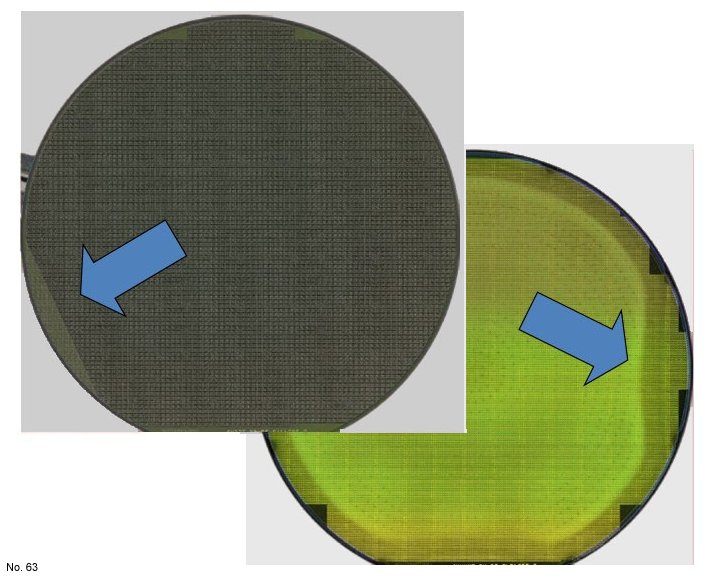
Figure 1: Above is an example of a blocked etch macro defect identified by EAGLEview where the semiconductor wafers were rotated from their normal semiconductor wafer position on an etch tool. The flat edge of the clamp covered the semiconductor wafers and then these areas did not receive a complete etch.
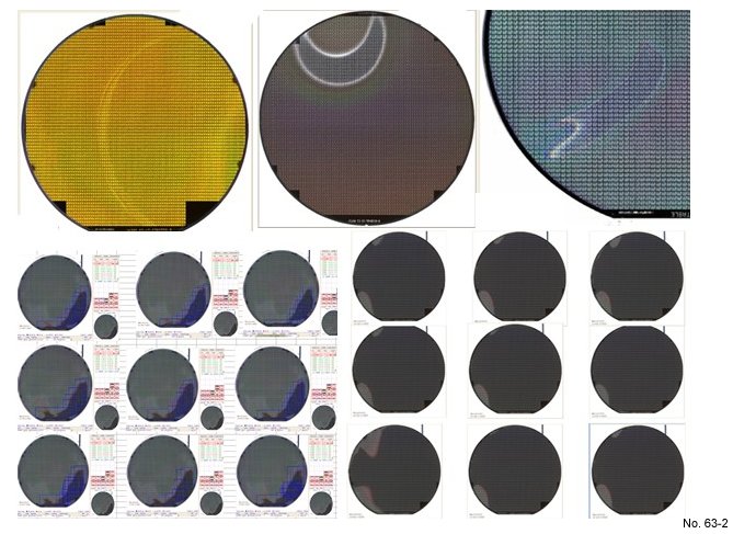
Figure 2: Blocked etch macro defect.