Alphabetical Index
Browse by Elements
Keyword Search
Dry Etchants
Dry and Wet Etchants
Wet Etchants
Bulk Etchants
Layer Etchants
Nano Etchants
Single Crystal Etchants
Thin Film Etchants
Thin Foil Etchants
Wafer Etchants
Al Etchants
Cd Etchants
Ga Etchants
Ge Etchants
In Etchants
New Etchants
Other Etchants
Si Etchants
Zn Etchants
Help
Home
Reticle Tilt Defect
Material Name: Wafer
Record No.: 63
Primary Chemical Element in Material: No data
Sample Type: Wafer
Uses: Etching
Etchant Name: None
Etching Method: Etching
Etchant (Electrolyte) Composition: No data
Procedure (Condition): No data
Note: EagleView easily spots reticle tilt semiconductor wafer defects which may look similar to lens wafer defects. Typically, a reticle tilt wafer macro defect goes across a stepper shot while a lens wafer macro defect tends to show a difference within the stepper shot. In this case, the center of the lens field is different than the edge of the lens field.
Reference: Website https://www.microtronic.com/defect-library/reticle-tilt-defect/, Image and text by courtesy of Microtronic company, 2020.
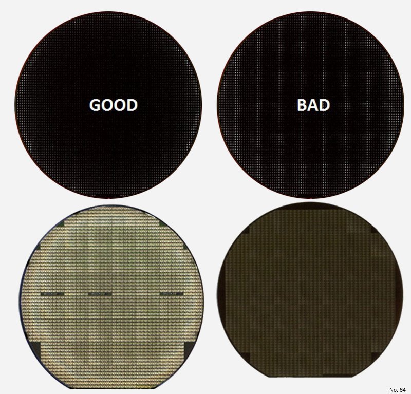
Figure 1: Above is an example of a blocked etch macro defect identified by EAGLEview where the semiconductor wafers were rotated from their normal semiconductor wafer position on an etch tool. The flat edge of the clamp covered the semiconductor wafers and then these areas did not receive a complete etch.