Alphabetical Index
Browse by Elements
Keyword Search
Dry Etchants
Dry and Wet Etchants
Wet Etchants
Bulk Etchants
Layer Etchants
Nano Etchants
Single Crystal Etchants
Thin Film Etchants
Thin Foil Etchants
Wafer Etchants
Al Etchants
Cd Etchants
Ga Etchants
Ge Etchants
In Etchants
New Etchants
Other Etchants
Si Etchants
Zn Etchants
Help
Home
Spin Defect – Entire Wafer
Material Name: Wafer
Record No.: 66
Primary Chemical Element in Material: No data
Sample Type: Wafer
Uses: Etching
Etchant Name: None
Etching Method: Etching
Etchant (Electrolyte) Composition: No data
Procedure (Condition): No data
Note: No data
Reference: Website https://www.microtronic.com/defect-library/spin-defect-entire-wafer/, Image and text by courtesy of Microtronic company, 2020.

Figure 1: This is a spin or coat macro defect which covers the entire semiconductor wafer. Without rework, this semiconductor wafer will most likely be scrapped. EagleView saves manufacturers time and money by identifying defects quickly — enabling faster corrective action.
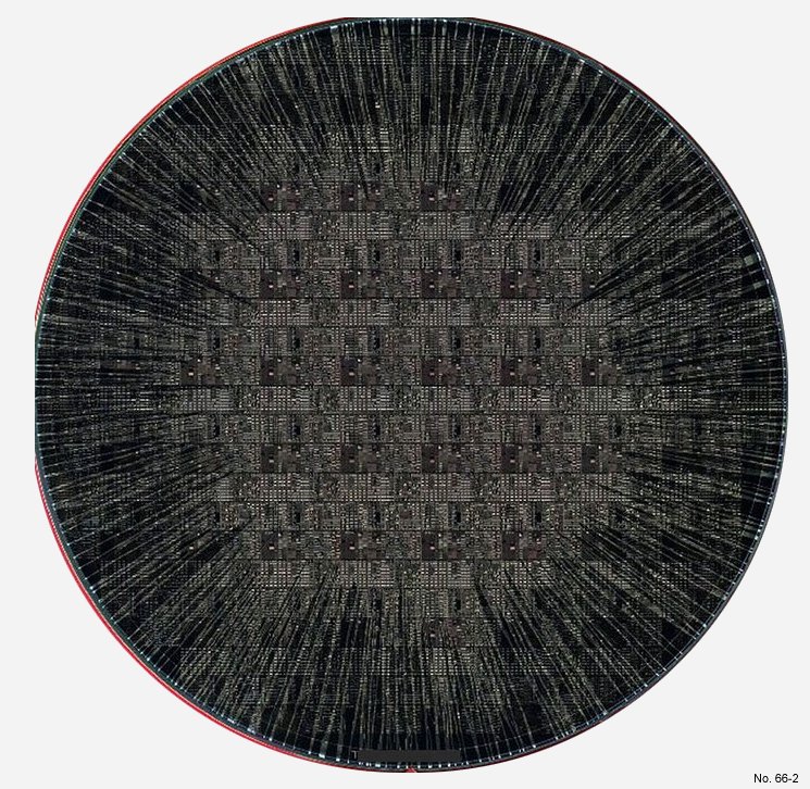
Figure 2: Example of a spin defect detected by EagleView due to a spin or coating issue in the semiconductor wafer production process.
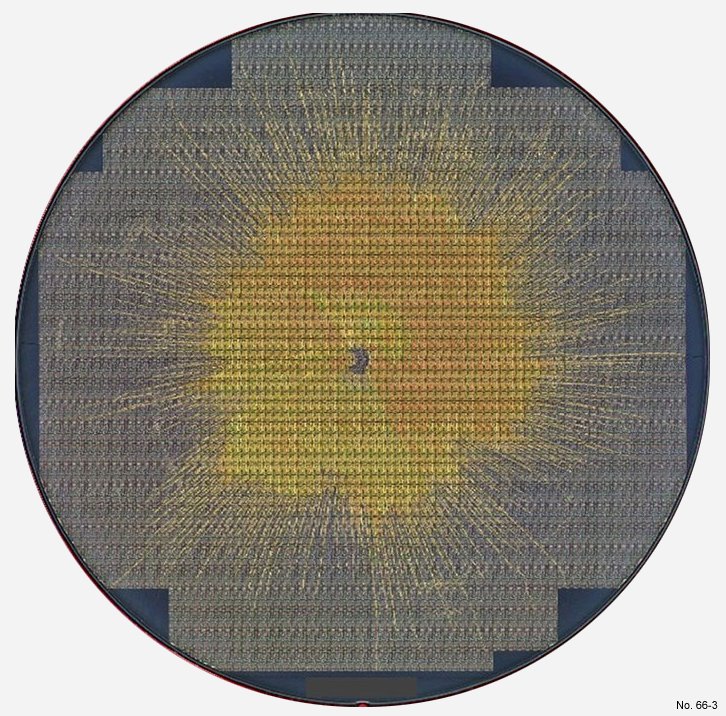
Figure 3: Spin or coat problem impacting the entire wafer. Without rework, this wafer will most likely be scrap. EagleView finds macro defects early while there is still time to take corrective action.