Alphabetical Index
Browse by Elements
Keyword Search
Dry Etchants
Dry and Wet Etchants
Wet Etchants
Bulk Etchants
Layer Etchants
Nano Etchants
Single Crystal Etchants
Thin Film Etchants
Thin Foil Etchants
Wafer Etchants
Al Etchants
Cd Etchants
Ga Etchants
Ge Etchants
In Etchants
New Etchants
Other Etchants
Si Etchants
Zn Etchants
Help
Home
Spin Defect on Edge
Material Name: Wafer
Record No.: 67
Primary Chemical Element in Material: No data
Sample Type: Wafer
Uses: Etching
Etchant Name: None
Etching Method: Etching
Etchant (Electrolyte) Composition: No data
Procedure (Condition): No data
Note: No data
Reference: Website https://www.microtronic.com/defect-library/spin-defect-entire-wafer/, Image and text by courtesy of Microtronic company, 2020.

Figure 1: Spin Defect on the edge of the semiconductor wafer is a coater issue that effects the semiconductor wafer edge. A spin defect appearing on the edge of the semiconductor wafer is typically due to lack of resist volume to sufficiently coat the entire wafer. This type of defect can also be caused by other process problems including topography process problems.
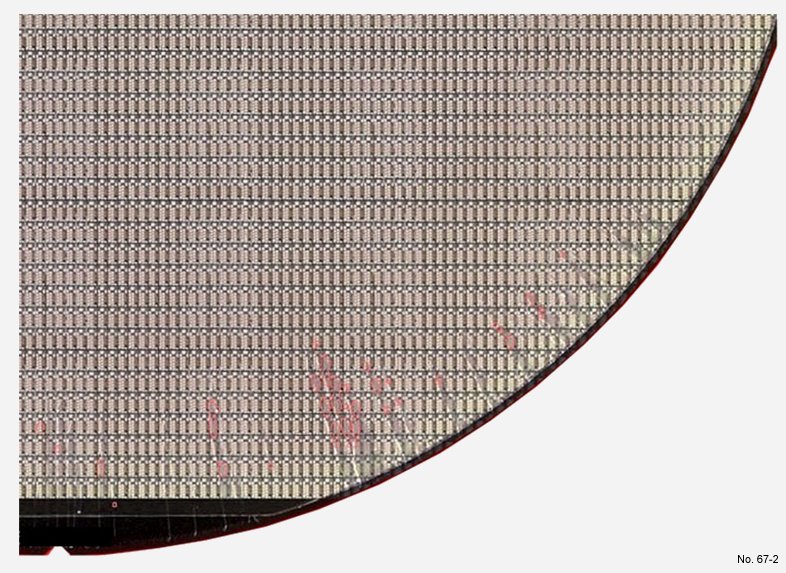
Figure 2: Here is another good example of a spin defect appearing on the edge of the Semiconductor wafer.
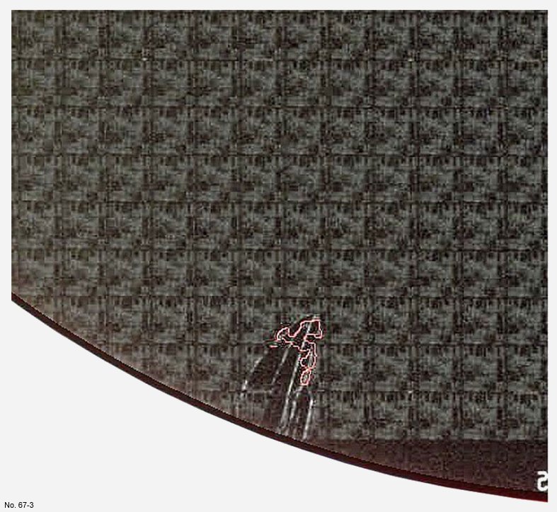
Figure 3: Another example of a spin defect on the edge of a semiconductor wafer. Note that in some instances, there may be only a single spin defect on a wafer.