Alphabetical Index
Browse by Elements
Keyword Search
Dry Etchants
Dry and Wet Etchants
Wet Etchants
Bulk Etchants
Layer Etchants
Nano Etchants
Single Crystal Etchants
Thin Film Etchants
Thin Foil Etchants
Wafer Etchants
Al Etchants
Cd Etchants
Ga Etchants
Ge Etchants
In Etchants
New Etchants
Other Etchants
Si Etchants
Zn Etchants
Help
Home
Center Spin Macro Defect
Material Name: Wafer
Record No.: 68
Primary Chemical Element in Material: No data
Sample Type: Wafer
Uses: Etching
Etchant Name: None
Etching Method: Etching
Etchant (Electrolyte) Composition: No data
Procedure (Condition): No data
Note: No data
Reference: Website https://www.microtronic.com/defect-library/center-spin-macro-defect/, Image and text by courtesy of Microtronic company, 2020.

Figure 1: Spin defects can occur anywhere on the wafer or throughout the entire wafer. This is an image of a spin macro defect that originated in the center of the semiconductor wafer. Spin macro defects in the center are usually due to air in the resist lines or a dirty nozzle tip that impedes the resist or causes sputtering at the start of the coat operation.
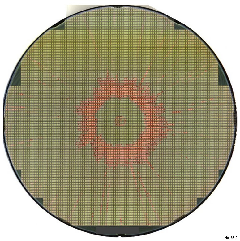
Figure 2: Some macro spin defects in the center of the semiconductor wafer can get quite large such as the example above.

Figure 3: The image above taken by EagleView is another good example of a spin defect originating in the center of the semiconductor wafer. EagleView allows you to measure the size of the defect and the percentage of the wafer impacted by the defect. In this case, the spin defect is less than 1% of the semiconductor wafer.