Alphabetical Index
Browse by Elements
Keyword Search
Dry Etchants
Dry and Wet Etchants
Wet Etchants
Bulk Etchants
Layer Etchants
Nano Etchants
Single Crystal Etchants
Thin Film Etchants
Thin Foil Etchants
Wafer Etchants
Al Etchants
Cd Etchants
Ga Etchants
Ge Etchants
In Etchants
New Etchants
Other Etchants
Si Etchants
Zn Etchants
Help
Home
Missing Patterns
Material Name: Wafer
Record No.: 77
Primary Chemical Element in Material: No data
Sample Type: Wafer
Uses: Etching
Etchant Name: None
Etching Method: Etching
Etchant (Electrolyte) Composition: No data
Procedure (Condition): No data
Note: No data
Reference: Website https://www.microtronic.com/defect-library/missing-patterns/, Image and text by courtesy of Microtronic company, 2020.

Figure 1: Missing pattern wafers can sometimes be seen in the thumbnail images that are generated in the EAGLEview software causing the semiconductor wafers to appear as a different color. Unpolished (CMP) semiconductor wafers also appear as missing pattern wafers.
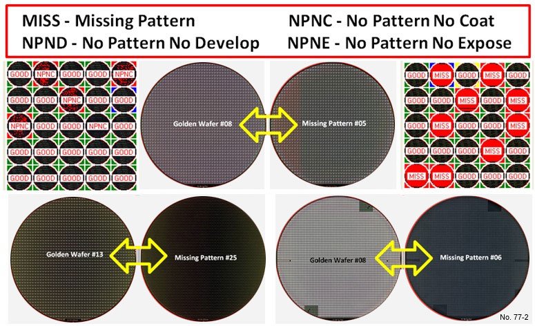
Figure 2: Some missing pattern wafers are very easy to detect as can be seen above on the thumbnail images from EAGLEview on the right. Other missing patterns on semiconductor wafers are more difficult to detect because the color differences are more subtle. These differences depend on the level (dark vs. bright), the cause of the missing pattern (lack of coat, expose or develop) and the throughout rate on the reticle.