Alphabetical Index
Browse by Elements
Keyword Search
Dry Etchants
Dry and Wet Etchants
Wet Etchants
Bulk Etchants
Layer Etchants
Nano Etchants
Single Crystal Etchants
Thin Film Etchants
Thin Foil Etchants
Wafer Etchants
Al Etchants
Cd Etchants
Ga Etchants
Ge Etchants
In Etchants
New Etchants
Other Etchants
Si Etchants
Zn Etchants
Help
Home
Crystalline Defects in Silicon
Material Name: Silicon
Record No.: 8
Primary Chemical Element in Material: Si
Sample Type: Wafer
Uses: Etching
Etchant Name: None
Etching Method: Wet etching
Etchant (Electrolyte) Composition: We have used P-type Boron doped mc-Si wafers of 10
x 10 cm2 in dimension and of about 1 Ohm x cm in electrical
resistivity. They were sawed from ingots grown by the
Heat Exchanger Method (HEM). In order to remove the
sawing process damage, we have begun by thinning and
polishing these wafers. During this step, we have used an
acidic polishing solution (known as “CP4 Etch”) made by
mixing nitric acid (HNO3), acetic acid (CH3COOH) and
hydrofluoric acid (HF) with respectively 50%, 30% and
20% concentrations. After 6 min of etching, we rinsed
thoroughly the mc-Si wafers with deionized water and
dried them under a nitrogen gun. In order to test the Secco
and Yang solutions, samples were cut from a polished mc-
Si wafer. Mainly, the etching time and the agitation mode
were varied. Before each delineation trial, the samples
were immersed in diluted HF (10%) solution for 30 seconds in order to remove the native silicon dioxide (SiO2) and then rinsed in deionized water. The Secco formulation is HF/potassium bichromate (K2Cr2O7)/H2O, obtained by mixing 2 parts of HF with 1 part of
K2Cr2O7/H2O at (0.15Moles) or (44 grams of K2Cr2O7 in
1litre of H2O). The Yang formulation is HF/chromic
acid (CrO3)/H2O, obtained by mixing 1 part of HF with 1
part of CrO3/H2O at (1.5 Moles) or (150 grams of CrO3 in
1 litre of H2O). After the Secco or Yang etching process
the samples were immediately rinsed in deionized water
and nitrogen dried. Subsequently, SEM observation and
other analysis have been performed.
Procedure (Condition): No data
Note:
The results of Yang and Secco delineation studies confirm
the revelation of crystalline defects for an immersion time
from 1 to 2 minutes, by clearly delineating dislocations,
twins, grain boundaries and dislocation lines. We observed
that dislocation pits etched with the Yang solution have
mainly triangular or quadratic forms, whereas the
dislocation pits are circular when using the Secco solution.
Figure 2 is an illustration of Secco defect delineation
process under the optimized conditions.
In order to compare the action of dislocation localization
between Secco and Yang solutions, we carried out a Secco
revelation on a sample previously revealed with Yang Etch
and vice-versa. The aim was to enable us to make a choice
between Secco and Yang Etches for the calculation of the
maximum density of defects. These tests showed that the
action of Secco is higher than Yang’s and lead us to
choose Secco for the calculation and mapping of
dislocation density. The profile of etched dislocation pits
revealed by this solution is shown on Figure 3. The
dipping time of the Secco delineation process was fixed at
5 minutes for the following defect mapping study. Such
dipping time removes 5 ìm of the dislocation zone as
shown by the SEM micrograph of Figure 3. This fine
knowledge and control of crystalline defect decoration by
“Secco Etch” on mc-Si wafers were directly applied to the
development of defect detection by the sheet resistance
variation technique.
Once the sheet resistance mapping of a polished mc-Si
wafer (10 x 10 cm2) was completed, we submitted the
wafer to a Secco etch during 5 minutes. We chose this
revelation time in order to strongly mark the defected
zones and thus obtain an appreciable variation of sheet
resistance. The mc-Si wafer revealed in this way was then
precisely placed under the 4 probes tester, and
measurement of the sheet resistance was carried out at the
initially selected positions. We plotted the mapping of
sheet resistance variation (delta R) on the 25 selected points
of the mc-Si wafer. The Figure 4 shows the layout
obtained for delta R. The next step was the superposition of
the physical image of decorated mc-Si wafer with that of
the delta R mapping. In order to accomplish this, we have
taken a digitalized photo of the whole Secco etched wafer
surface, scaled it, and finally successfully superposed it to
delta R mapping. The Figure 4 illustrates this original result.
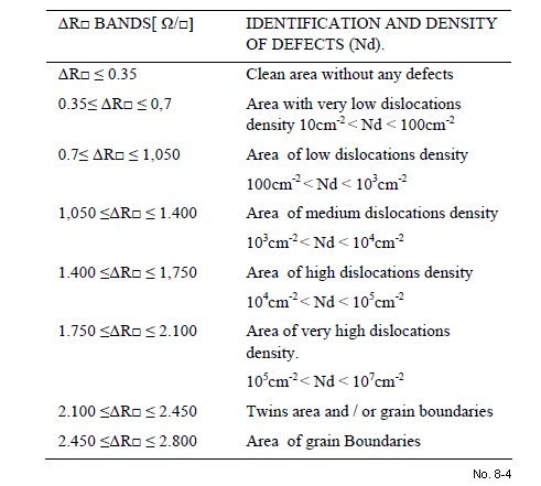
The SEM analysis of these results allowed us to make the
first classification for delta R bands according to the revealed
crystalline defect type and average dislocation density.
This classification is summarized on Table 1.
Reference: Mohamed FATHI, Ahmed CHIKOUCHE, New Method for Quality Evaluation of Mc-Si Wafers Implied in
the Fabrication of Photovoltaic Cells, Jordan Journal of Mechanical and Industrial Engineering, Volume 4, Number 1, Jan. 2010, pp. 151 - 154.

Figure 2: Secco defects delineation on mc-Si.

Figure 3: Cross section of dislocation delineated by Secco Etch for
5 minutes.

Figure 4: Superposition of the physical image of the defects area with delta R mapping.
Table 1: Classification of defects types according to sheet resistance variation bands.