Alphabetical Index
Browse by Elements
Keyword Search
Dry Etchants
Dry and Wet Etchants
Wet Etchants
Bulk Etchants
Layer Etchants
Nano Etchants
Single Crystal Etchants
Thin Film Etchants
Thin Foil Etchants
Wafer Etchants
Al Etchants
Cd Etchants
Ga Etchants
Ge Etchants
In Etchants
New Etchants
Other Etchants
Si Etchants
Zn Etchants
Help
Home
Flashfield Defects
Material Name: Wafer
Record No.: 81
Primary Chemical Element in Material: No data
Sample Type: Wafer
Uses: Etching
Etchant Name: None
Etching Method: Etching
Etchant (Electrolyte) Composition: No data
Procedure (Condition): No data
Note: No data
Reference: Website https://www.microtronic.com/defect-library/flashfield-defects/, Image and text by courtesy of Microtronic company, 2020.
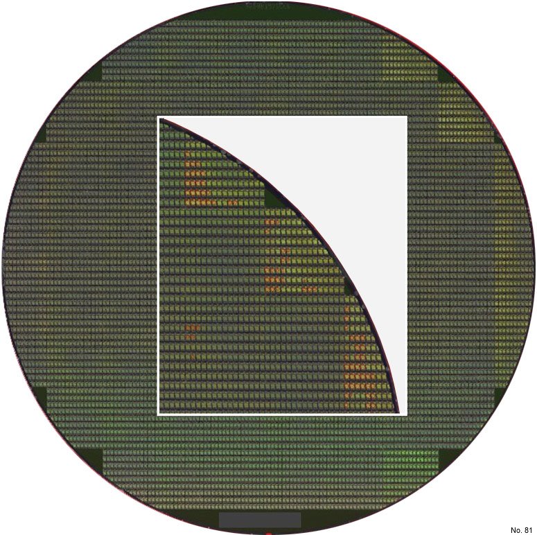
Figure 1: Flash field defects are typically near the edge of the semiconductor wafer and due to a focus isssue for a stepper shot or possibly a topography issue.
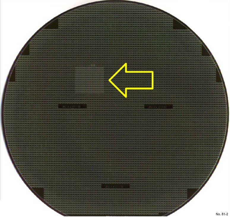
Figure 2: Some flash field macro defects may occur in the interior of the wafer – these macro defects are also referred to as a dropped or missing shot.
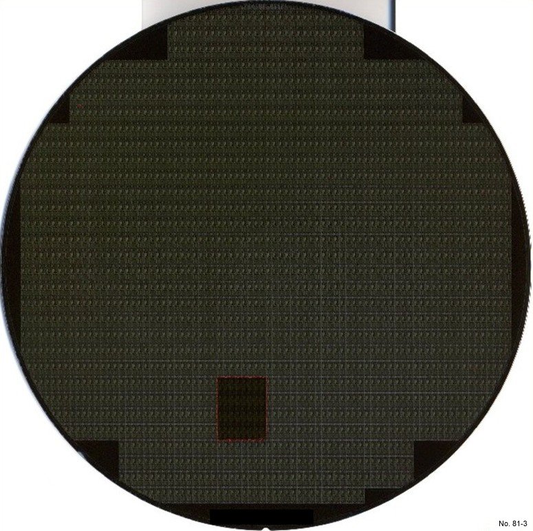
Figure 3: Additional example of a flash field defect on the semiconductor wafer.

Figure 4: Additional example of a flash field macro defect on the semiconductor wafer.