Alphabetical Index
Browse by Elements
Keyword Search
Dry Etchants
Dry and Wet Etchants
Wet Etchants
Bulk Etchants
Layer Etchants
Nano Etchants
Single Crystal Etchants
Thin Film Etchants
Thin Foil Etchants
Wafer Etchants
Al Etchants
Cd Etchants
Ga Etchants
Ge Etchants
In Etchants
New Etchants
Other Etchants
Si Etchants
Zn Etchants
Help
Home
Wafer Contamination – Small
Material Name: Wafer
Record No.: 85
Primary Chemical Element in Material: No data
Sample Type: Wafer
Uses: Etching
Etchant Name: None
Etching Method: Etching
Etchant (Electrolyte) Composition: No data
Procedure (Condition): No data
Note: No data
Reference: Website https://www.microtronic.com/defect-library/wafer-contamination-small/, Image and text by courtesy of Microtronic company, 2020.
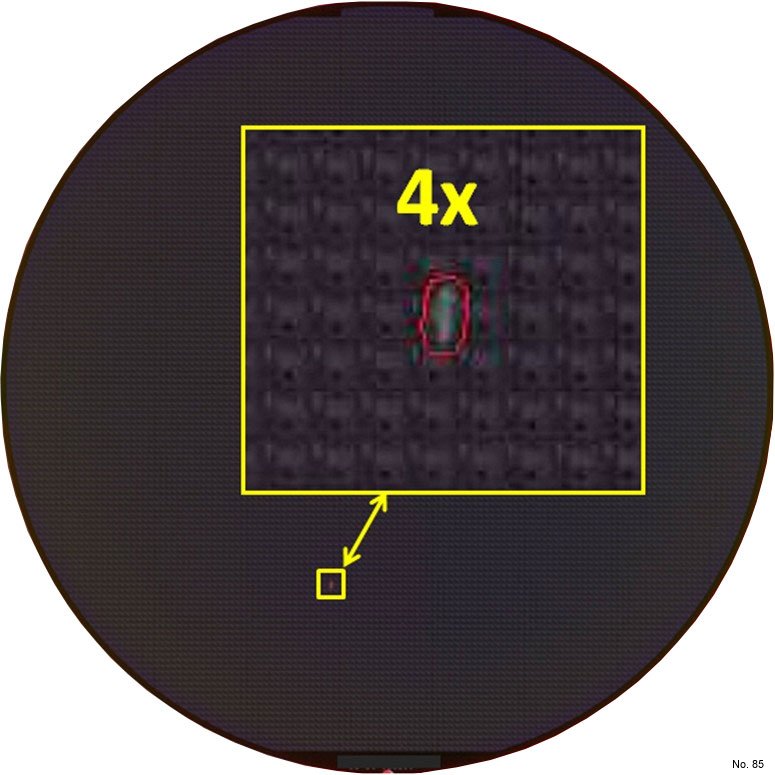
Figure 1: EAGLEview detects small contamination defects on the semiconductor wafer instantly. Typically, any small semiconductor wafer defect that is not a scratch or particle might be considered a small contamination macro defect. The image above shows a small contamination semiconductor wafer macro defect magnified 4x.

Figure 2: Example of a small contamination semiconductor wafer macro defect. Image magnified 8x.

Figure 3: An additional example of a semiconductor wafer macro defect caused by small contamination. Image magnified 4x.
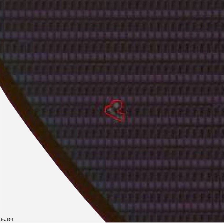
Figure 4: An additional example of a semiconductor wafer macro defect picked up by EAGLEview caused by small contamination in the production process. Image magnified 8x.