Alphabetical Index
Browse by Elements
Keyword Search
Dry Etchants
Dry and Wet Etchants
Wet Etchants
Bulk Etchants
Layer Etchants
Nano Etchants
Single Crystal Etchants
Thin Film Etchants
Thin Foil Etchants
Wafer Etchants
Al Etchants
Cd Etchants
Ga Etchants
Ge Etchants
In Etchants
New Etchants
Other Etchants
Si Etchants
Zn Etchants
Help
Home
Wafer Contamination – Large
Material Name: Wafer
Record No.: 86
Primary Chemical Element in Material: No data
Sample Type: Wafer
Uses: Etching
Etchant Name: None
Etching Method: Etching
Etchant (Electrolyte) Composition: No data
Procedure (Condition): No data
Note: No data
Reference: Website https://www.microtronic.com/defect-library/wafer-contamination-large/, Image and text by courtesy of Microtronic company, 2020.

Figure 1: An example of a large contamination macro defect found by EAGLEview on a semiconductor wafer that has an irregular shape.

Figure 2: An additional example of a semiconductor wafer macro defect caused by contamination.
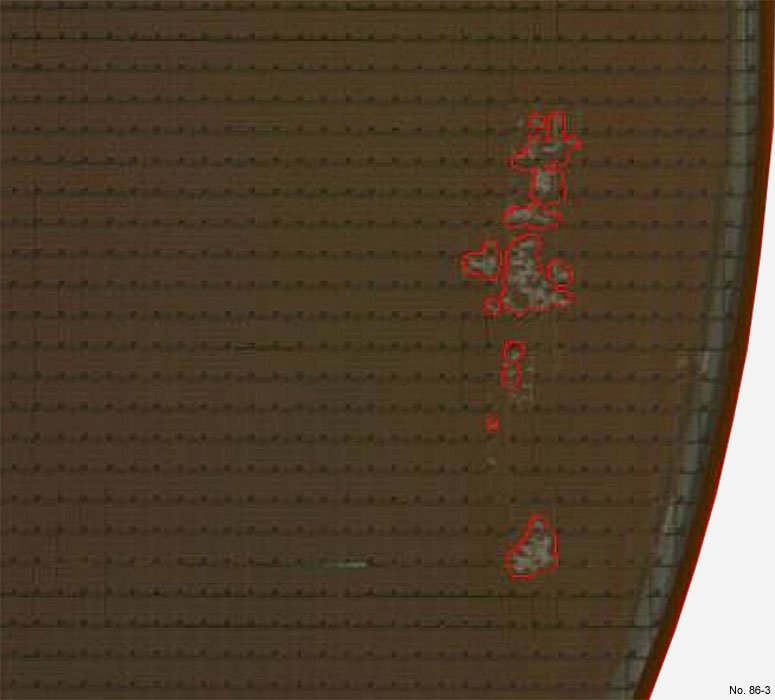
Figure 3: EAGLEview image depicting a large contamination macro defect on the semiconductor wafer.
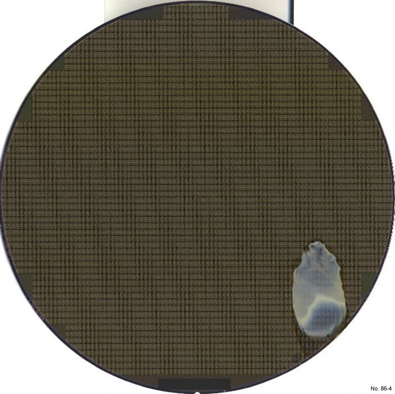
Figure 4: Large contamination macro defect detected by EAGLEview on semiconductor wafer.