Alphabetical Index
Browse by Elements
Keyword Search
Dry Etchants
Dry and Wet Etchants
Wet Etchants
Bulk Etchants
Layer Etchants
Nano Etchants
Single Crystal Etchants
Thin Film Etchants
Thin Foil Etchants
Wafer Etchants
Al Etchants
Cd Etchants
Ga Etchants
Ge Etchants
In Etchants
New Etchants
Other Etchants
Si Etchants
Zn Etchants
Help
Home
Edge Chips – Macro Defects
Material Name: Wafer
Record No.: 88
Primary Chemical Element in Material: No data
Sample Type: Wafer
Uses: Etching
Etchant Name: None
Etching Method: Etching
Etchant (Electrolyte) Composition: No data
Procedure (Condition): No data
Note: No data
Reference: Website https://www.microtronic.com/defect-library/edge-chips-macro-defects/, Image and text by courtesy of Microtronic company, 2020.

Figure 1: Above is an example of a semiconductor wafer edge chip defect detected by EAGLEview. Note that a white circle around the semiconductor wafer indicates that an edge defect may have been detected. The semiconductor wafer edge ribbon will also indicate the wafer defect location based on 360 degrees with the flat or notch at 0 degrees. EAGLEview makes it easy to visualize and clearly see where the wafer defect resides.
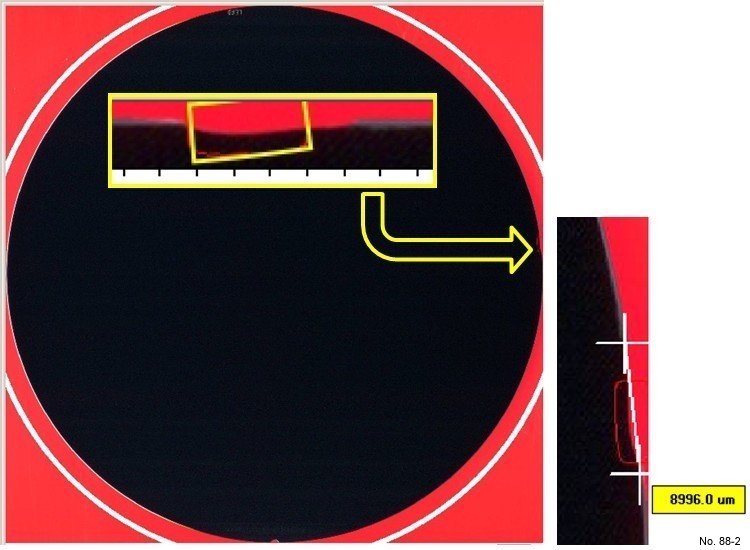
Figure 2: On the far right side of the semiconductor wafer is an edge chip defect. Microtronic’s EAGLEview system’s measuring tool indicates that this semiconductor wafer edge chip defect is about 9 mm long.
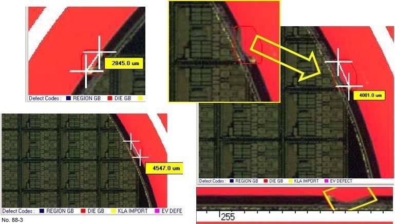
Figure 3: Additional examples of semiconductor wafer edge chip defects detected by EAGLEview.