Alphabetical Index
Browse by Elements
Keyword Search
Dry Etchants
Dry and Wet Etchants
Wet Etchants
Bulk Etchants
Layer Etchants
Nano Etchants
Single Crystal Etchants
Thin Film Etchants
Thin Foil Etchants
Wafer Etchants
Al Etchants
Cd Etchants
Ga Etchants
Ge Etchants
In Etchants
New Etchants
Other Etchants
Si Etchants
Zn Etchants
Help
Home
Pyrex Glass Wafer - Defects Observed on the Etched Glass Surface
Material Name: Pyrex glass wafer
Record No.: 9
Primary Chemical Element in Material: Si
Sample Type: Wfer
Uses: Etching
Etchant Name: None
Etching Method: Wet etching
Etchant (Electrolyte) Composition: No data
Procedure (Condition): No data
Note: This paper addresses the main issues related to wet
micromachining of one of the mostly used
BioMEMS materials - glass - and proposes two
optimized solutions for deep wet etching. As a
result, 500 µm-thick Pyrex glass wafer was etched
using an etching mask consisting of low stress
amorphous silicon (a:Si) and photoresist. Moreover
we report the successful through etching of 1mm
Pyrex glass wafer using a combination of low stress
a:Si/SiC/photoresist mask.
There are two types of defects in the glass etching
process: pinholes and notching defects on the
edges. These can be observed after certain etch
time, and are the result of the interaction between
the etchant and mask. Figure 1 illustrates these
defects. The main reasons of defect generation are:
- residual stress in the masking layer,
- stress type (tensile or compressive),
- stress gradient existing in multilayer mask,
- hydrophilicity of the surface.
The residual stress, as we mentioned in ref., has a
strong influence on the defect generation. The small
defects on the surface are generated during masking
layer depositions. If the stress is tensile, the residual
stress generates small microchannels in the masking
layer. If the masking layer surface is hydrophilic
the etching solution will be “sucked” in these
microchannels. As a consequence, pinholes will
start to generate in a short time. For this reason, a
masking layer with compressive stress, which
commonly exists in amorphous silicon or
polysilicon, is sometimes preferred.
The existence of notching defects on the edges is a
typical characteristic of metal masks such as Cr/Au
and Cr/Cu that present tensile stress as high as 1
GPa. These notching defects are generated due to
the stress gradient or the breakage of the edge
of the mask. During isotropic etching process, due
to underetching, the edge of masking layer becomes
a freestanding structure. Due to the stress and/or
stress gradient, the mask can break and leave some
areas uncovered.
Hydrophilic or hydrophobic property of the
masking layer surface, as we previously mentioned,
also play an important role. A small defect, for
example micro-creeps on a hydrophobic surface, is
very difficult to be filled with the etching solution,
resulting in a better etching protection. For this
reason, amorphous silicon or polysilicon, as same
as silicon, presents a hydrophobic behavior and is
preferred to be used as etching mask layer
compared to Cr/Au mask.
Reference: Ciprian Iliescu, Bangtao Chen and Jianmin Miao, DEEP WET ETCHING-THROUGH 1 mm PYREX GLASS WAFER
FOR MICROFLUIDIC APPLICATIONS, February 2007, Proceedings of the IEEE International Conference on Micro Electro Mechanical Systems (MEMS), DOI: 10.1109/MEMSYS.2007.4433150.
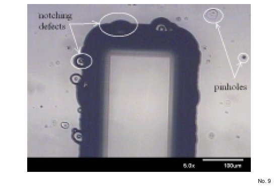
Figure 1: Defects observed on the etched glass surface.