Alphabetical Index
Browse by Elements
Keyword Search
Dry Etchants
Dry and Wet Etchants
Wet Etchants
Bulk Etchants
Layer Etchants
Nano Etchants
Single Crystal Etchants
Thin Film Etchants
Thin Foil Etchants
Wafer Etchants
Al Etchants
Cd Etchants
Ga Etchants
Ge Etchants
In Etchants
New Etchants
Other Etchants
Si Etchants
Zn Etchants
Help
Home
Overlay Shift
Material Name: Silicon
Record No.: 99
Primary Chemical Element in Material: Si
Sample Type: Wafer
Uses: Etching
Etchant Name: None
Etching Method: Dry etching
Etchant (Electrolyte) Composition: No data
Procedure (Condition): No data
Note: For wafer-edge detractors, electrical
failure analysis can provide only limited
infor mation due to super position
of process issues from more layers
compared to wafer center. Extensive
rever se eng ineer ing is required,
especially if process issues or defects are
non-detectable inline. Additional delays
are caused if analysis has to be carried out in serial mode, in a similar fashion
to archaeolog ical digs uncover ing
the buried achievements of ancient
civilizations layer by layer. Figure 1
shows an example of debugging of
multiple process issues at an edge die.
Initially, only the cluster bitline fail
was observed electrically; physical failure
analysis indicated that it was due to a
local contact-to-bitline (C1-M0) overlay
shift. Within the affected die no overlay
shift was present towards wafer center.
Statistical analysis confirmed a baseline
issue for the given die which, once
fixed by appropriate overlay correction,
showed failures in master data lines
(MDQ) in the electrical fail signature.
Physical failure analysis revealed that the
observed MDQ fail was associated with
back-end-of-line metallization contact
(C2) opens. The defects were optically
non-visible by inline defect inspection.
Hence, a voltage contrast-based e-
Beam defect inspection was developed
for inline monitoring, while the issue
was addressed using blading adjustment
for the extreme edge shot. Finally,
single cell fails were detected, caused by
a localized active-area to deep-trench
capacitor (AA-DT) overlay shift at the
extreme edge of the affected die. The
cause of these fails could be attributed
to shifted DTs due to plasma distortion
dur ing hard-mask open process.
Eventually, the process uniformity could
be further optimized by a redesign of the etch tool. Learning cycles could be
further reduced by use of the Automated
Process Inspection (API) feature of
the SEM review tool. A specifically
designed API recipe provided inline
information on AA/DT overlay shift
right after AA etch in this case, which
negated the need for waiting for the
electrical test to verify the process fix.
Reference: Oguz Yavas, Ernst Richter, Christian Kluthe & Markus Sickmoeller, Wafer-edge yield engineering in
leading-edge DRAM manufacturing, Semiconductor Fabtech -39th Edition, www.fabtech.org, 2009, pp. 1-5.
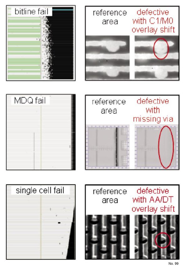
Figure 1: Electrical fail signatures (left) and SEM images (right) of defects for a failing
wafer-edge die.