Alphabetical Index
Browse by Elements
Keyword Search
Dry Etchants
Dry and Wet Etchants
Wet Etchants
Bulk Etchants
Layer Etchants
Nano Etchants
Single Crystal Etchants
Thin Film Etchants
Thin Foil Etchants
Wafer Etchants
Al Etchants
Cd Etchants
Ga Etchants
Ge Etchants
In Etchants
New Etchants
Other Etchants
Si Etchants
Zn Etchants
Help
Home
Semiconductor Defects - Figure Browser
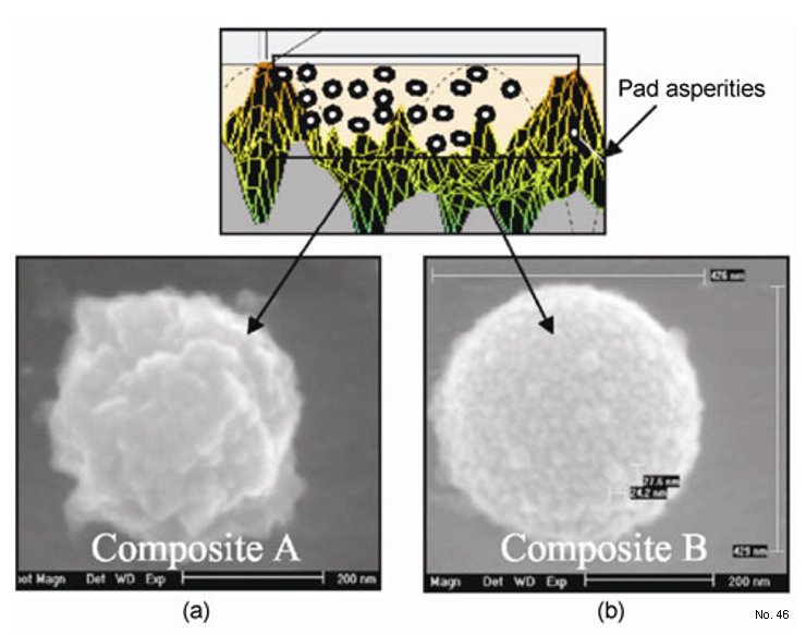
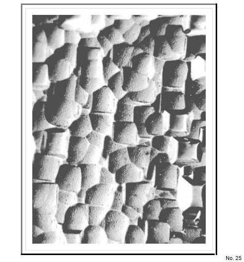
µ-Scale Phenomen During CMP

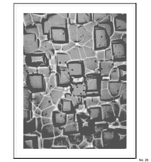
2 Chamber Macro Defect

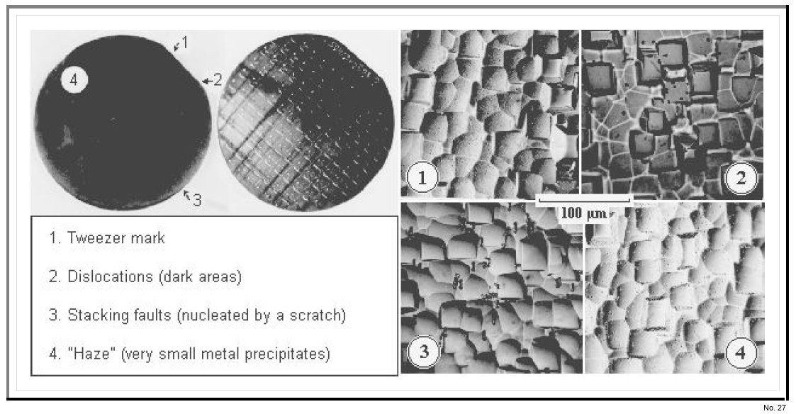
3 Chamber Macro Defect
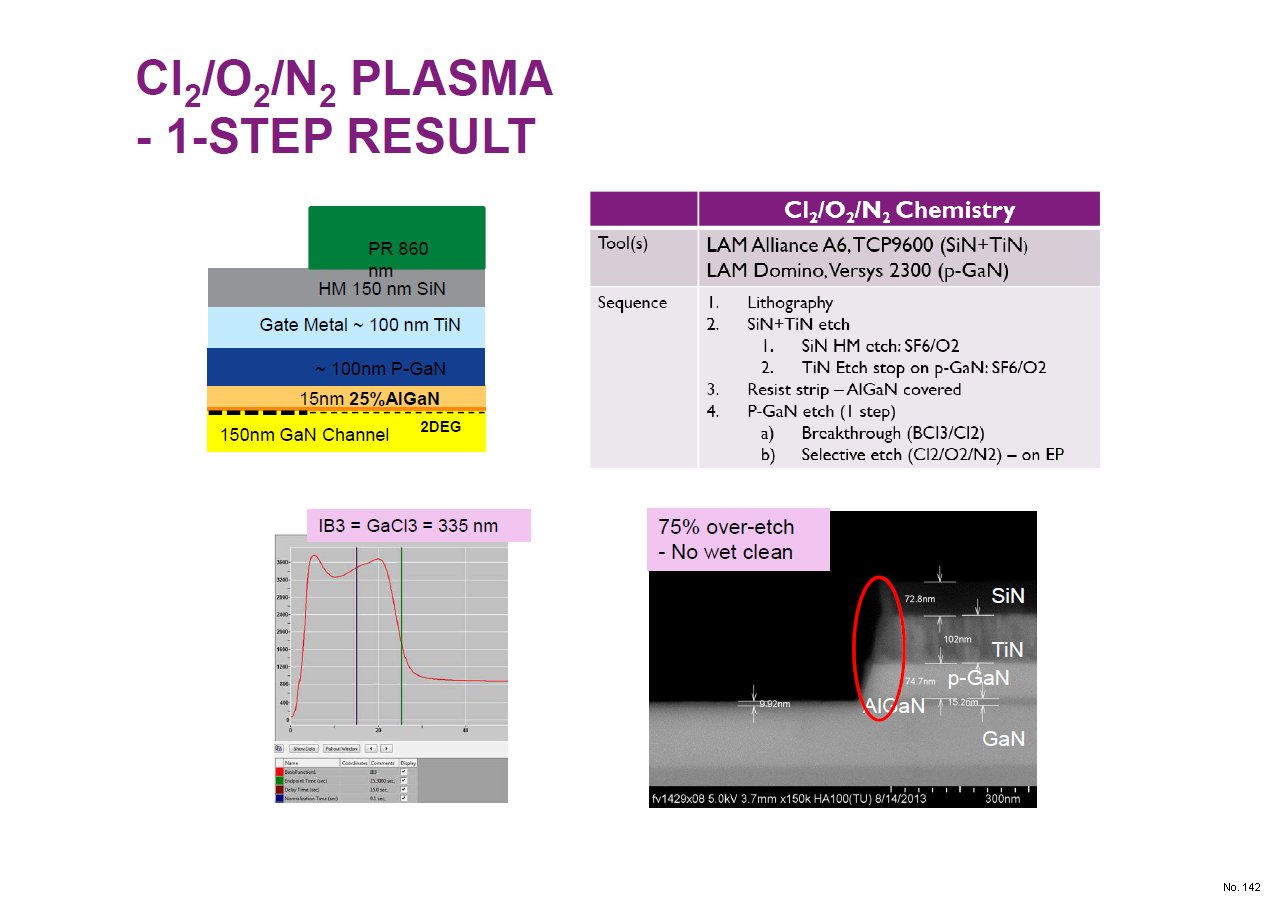
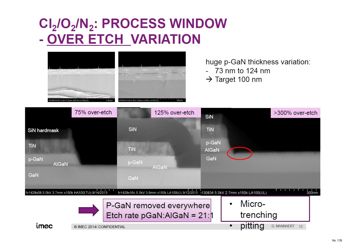
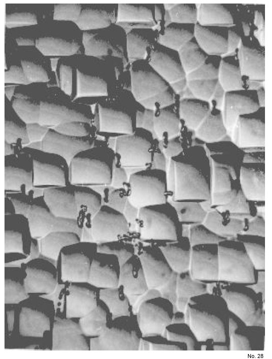
75% Over Etch - GaN

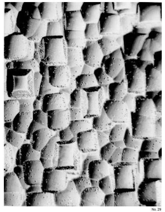
Aluminum Corrosion - Dry etching
Amorphous Silicon Spikes
Arcing Defects
Arcing Generated Aluminum Particle on Wafer Surface

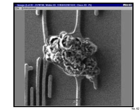
Au Shorting Two Wires
Backside Contamination

Bevel Etch
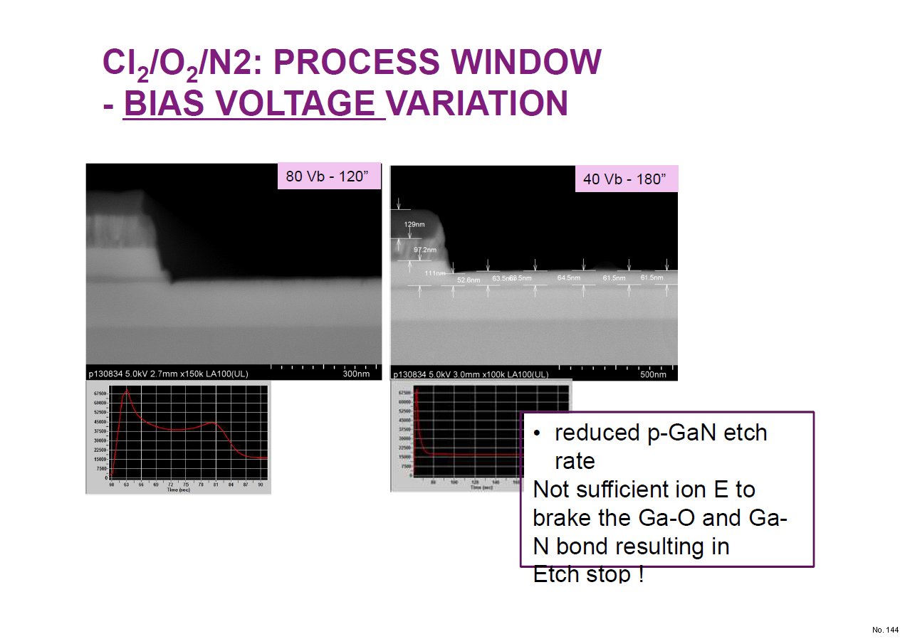
Bias Voltage Variation - GaN
Blocked Etch Macro Defect
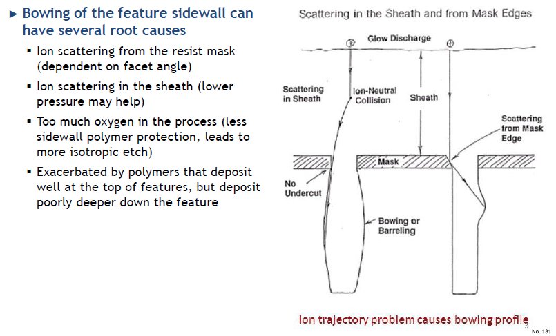
Bowing
Breakdown in Vertical Gate Oxide
CMP – Macro Defects
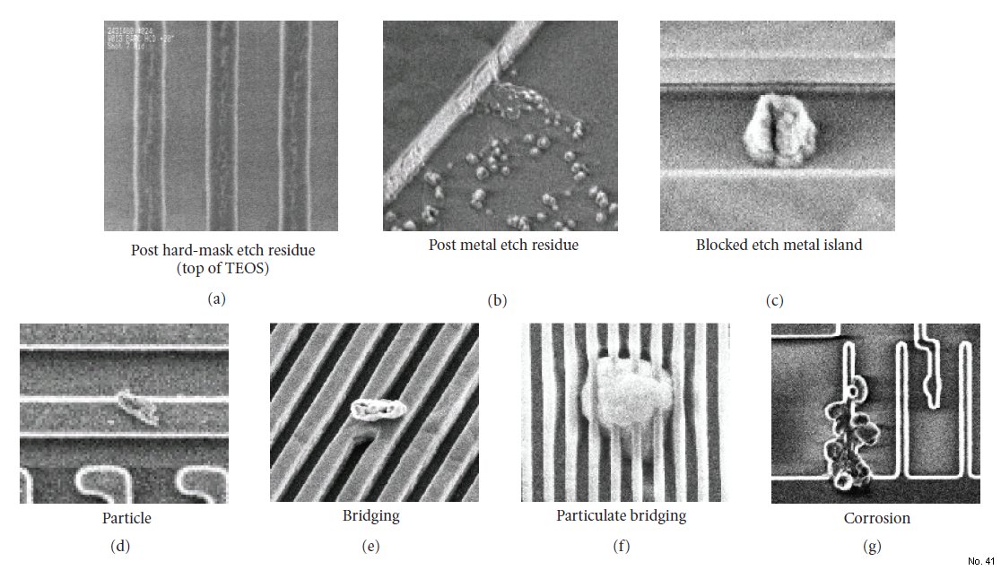
CMP-Induced Defects
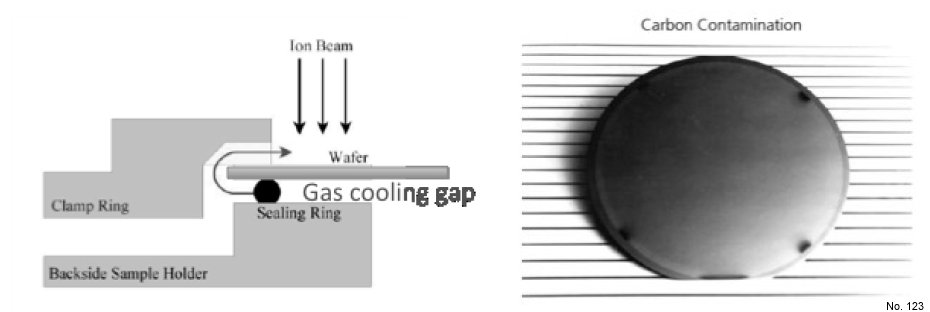
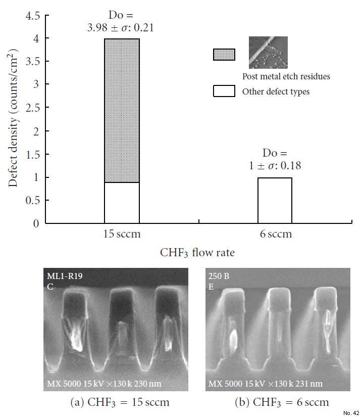
Carbon Contamination
Categories of Different Types of Scratches
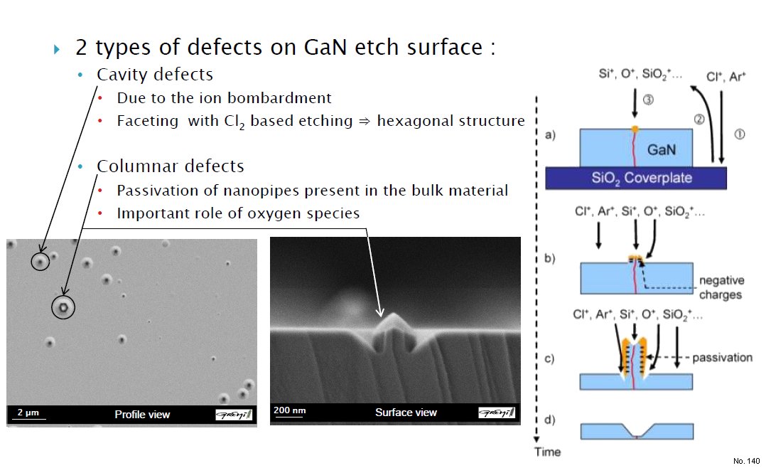
Cavity Defects, Columnar Defects - GaN

Center Spin Macro Defect

Charge Losses for VB Grown CdMnTe Detector
Chatter Surface Damage

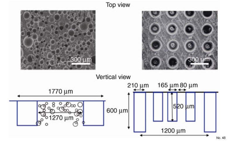
Contaminants Over the Substrate Surface

Cooper Voids, Silicon Micrograss
Corner Cavity in Collector Mesa

Corrosion of Au Plated Connector

Cr/Au film Peeling

Crack in Aramid Fiber/Epoxy Matrix Interface

Crystalline Defects in Silicon

Damaged Layer
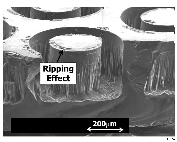
Defect in Digital Micromirror Device
Defects in Transistors Revealed by Etching

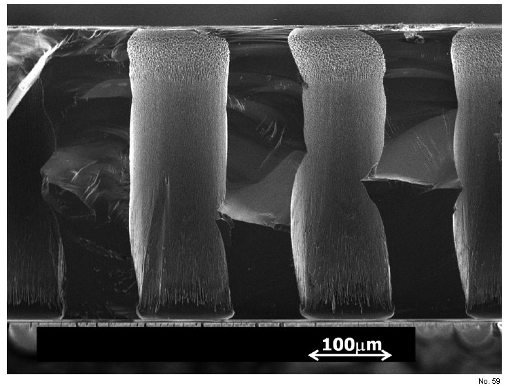
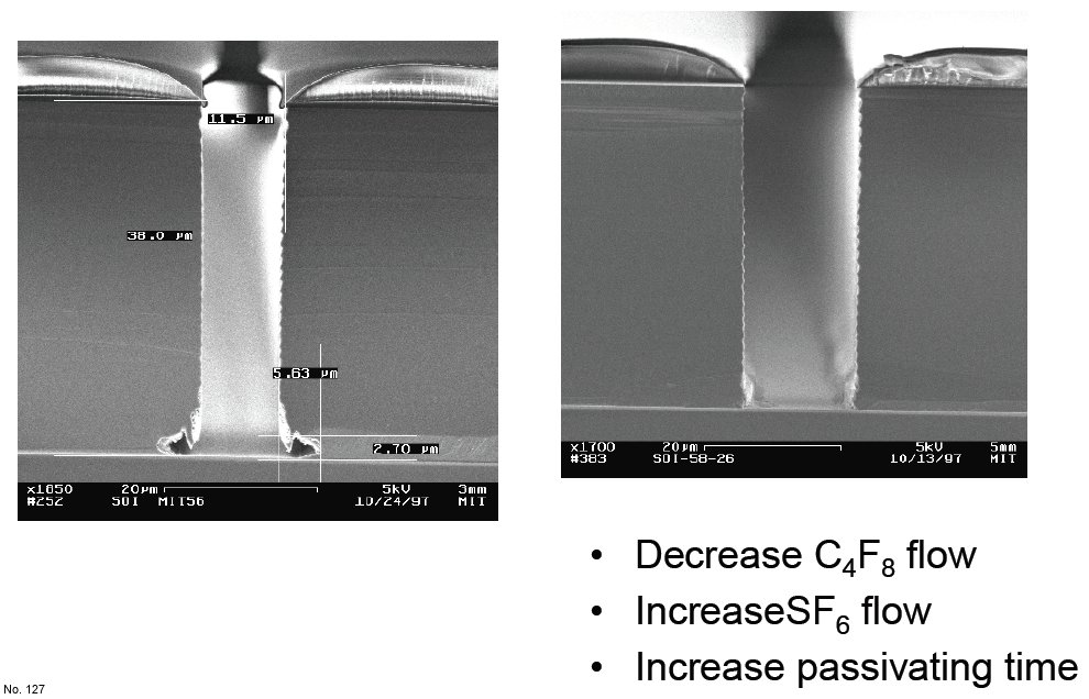
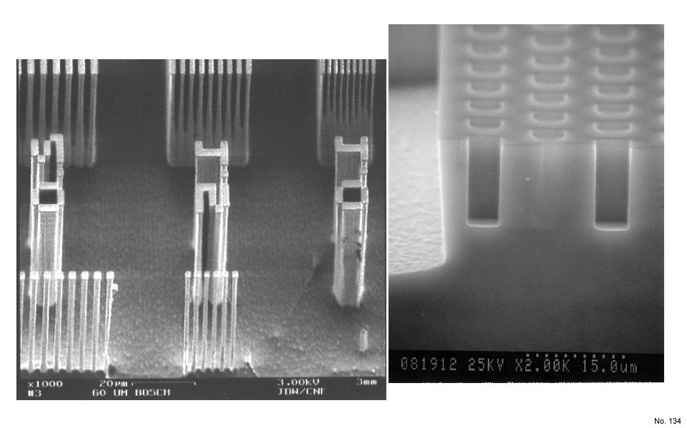
Degradation Caused by Excessive Cycle Times During Bosch Process
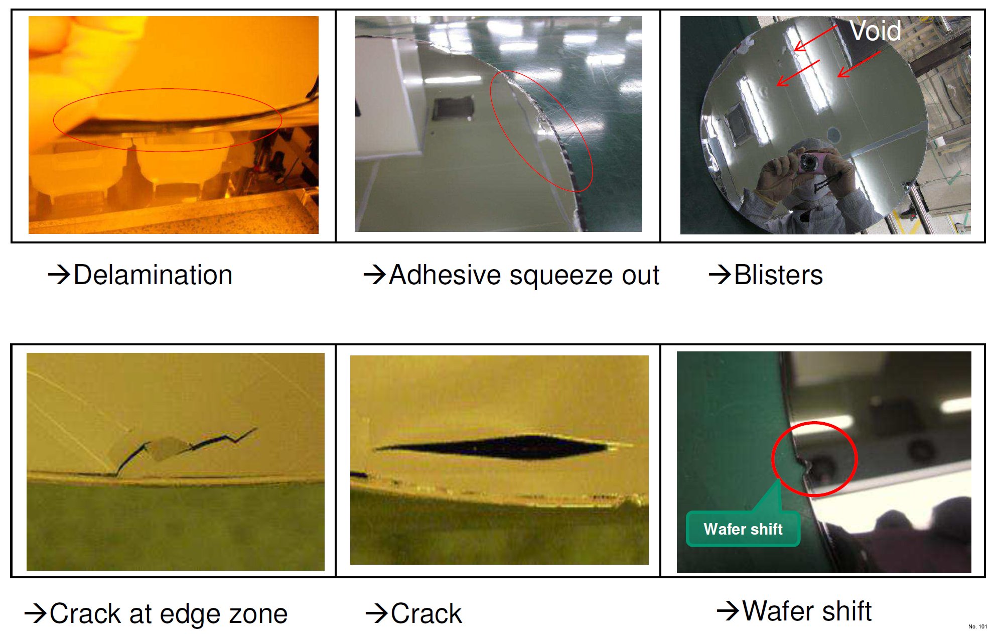
Delamination, Adhesive Squeeze Out, Blisters, Crack at Edge Zone, Crack, Wafer Shift
Developer Related Defects

Dishing and Erosion
Dislocations

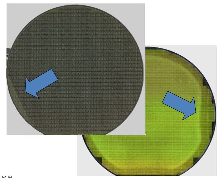
Distorted Oxide Hard Mask Patterns

Dual Damascene Structure - Copper Wafer
EBR Drip Defect

Edge Chips – Macro Defects

Etch Pattern of Swirl Defects in Silicon
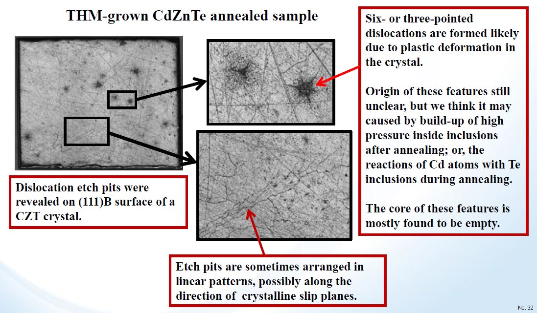
Etch Pits Revealed in CdZnTe THM-Grown Sample

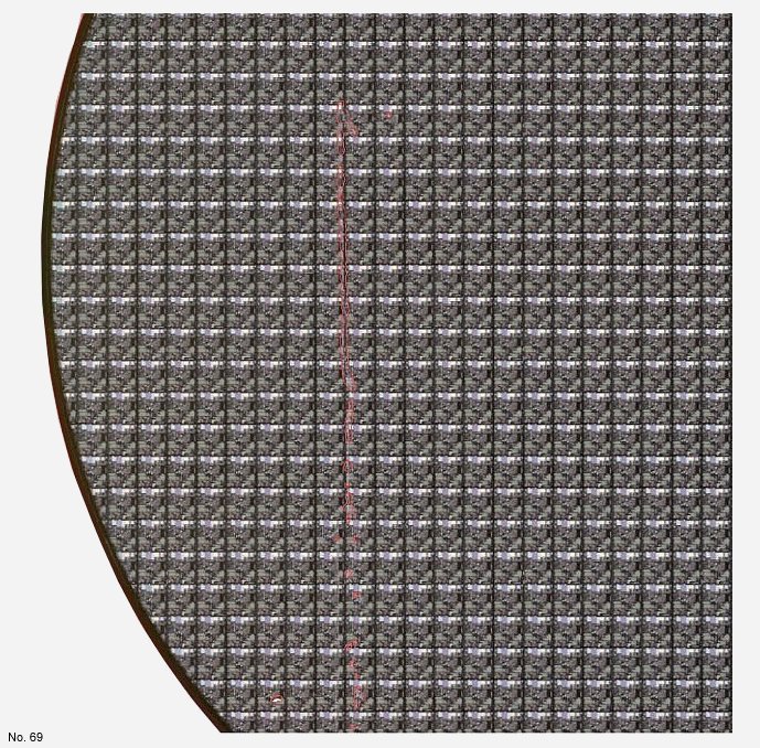
Etch induced damage for different processes - HgCdTe

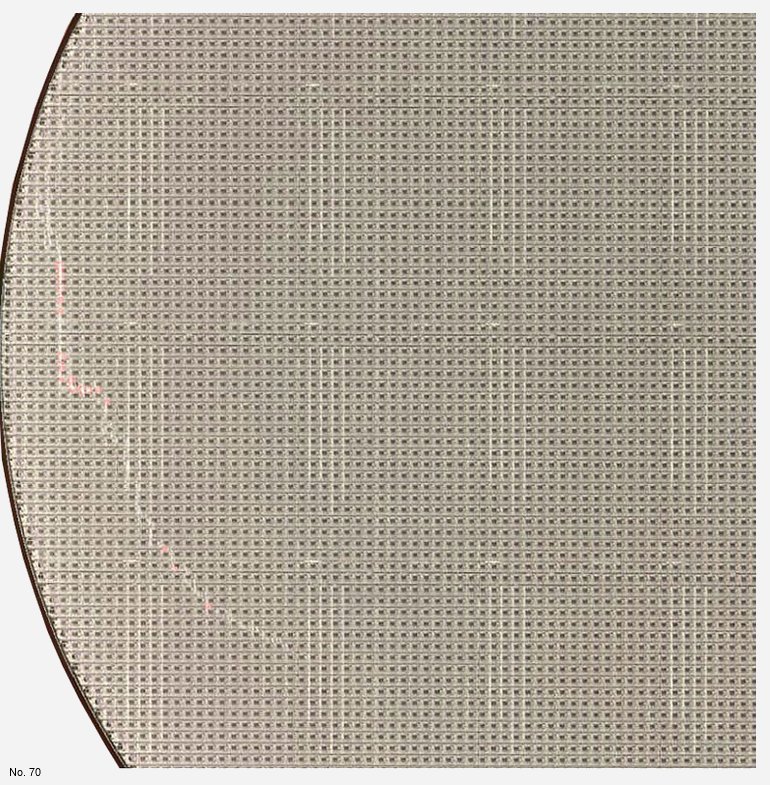
Evidence of Charge Losses by Star-Shaped Features - CdZnTe
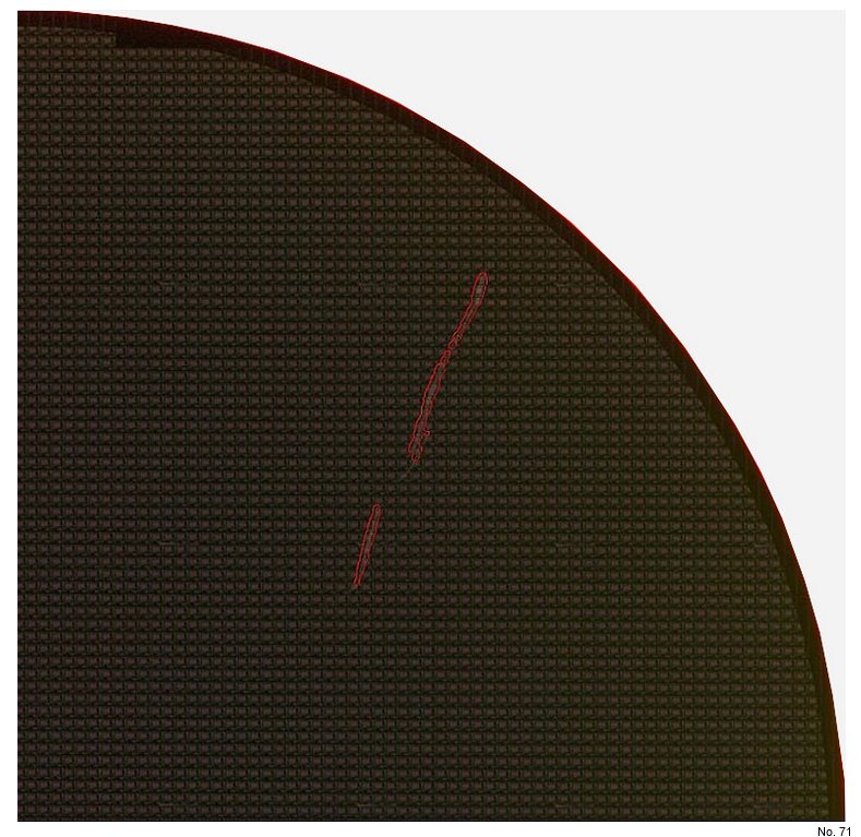
Example of Notching and Bowing Occuring in an Etched Sample
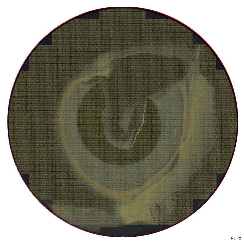
Example of an Unsuccessful Cr Lift Off
Examples of Defect Adders Within the Oxide-Masked Al Etching Process Sequence
Faceting
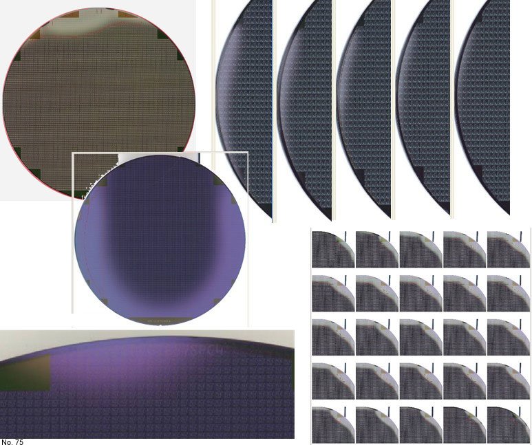
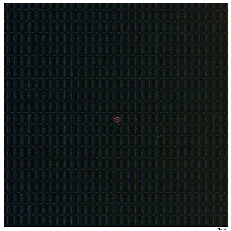
Faceting/Trenching/Sidewall Taper

Failure Modes IKnduced by Tin Whiskers

FexOy Particles
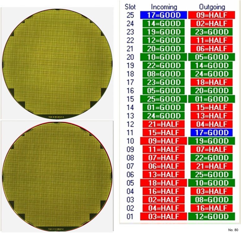
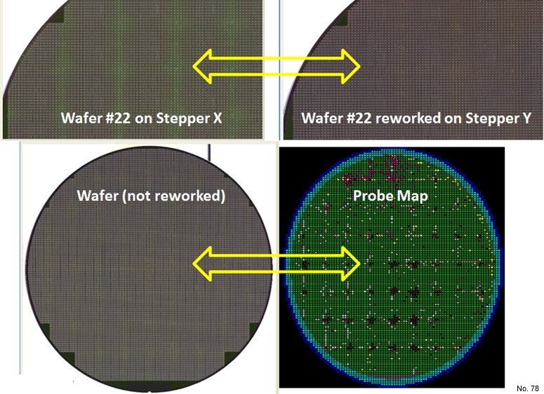
First 12 Wafers – Different
Flashfield Defects
Fluorine Contamination
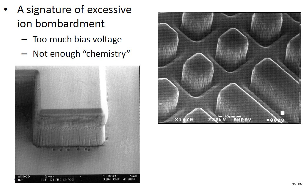
Footing Effect
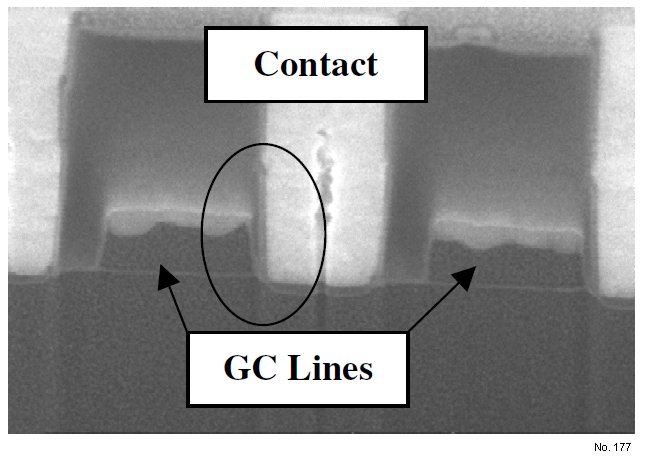
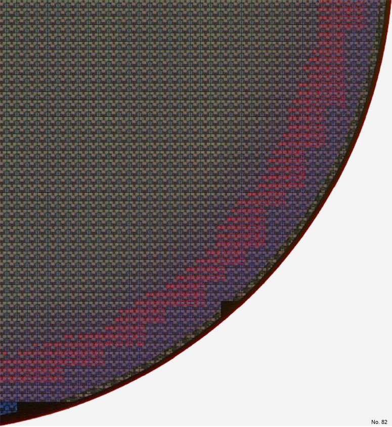
Gate Conductor (GC) Short
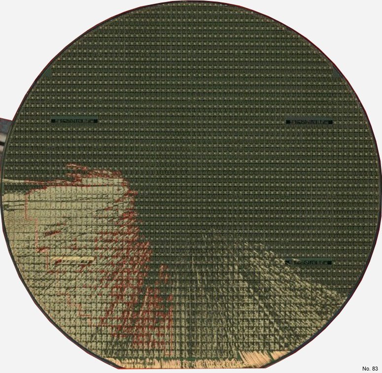
Gate Oxide Defects
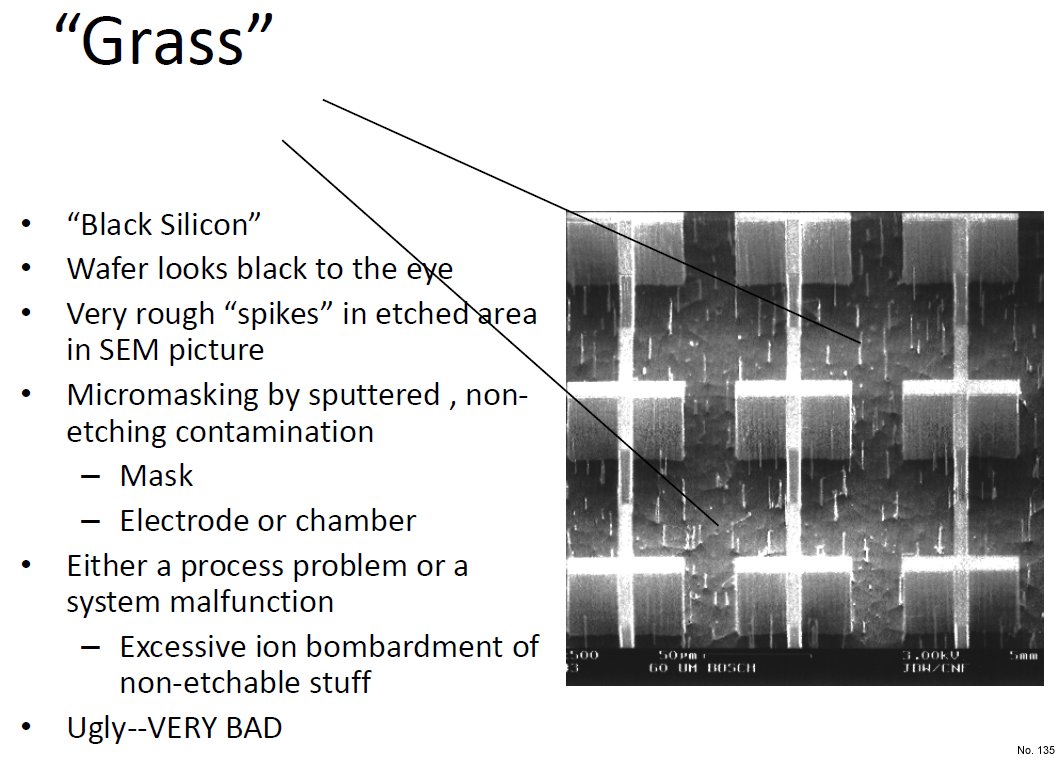
Grass
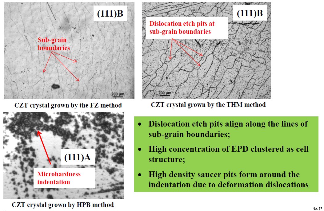
Grown-in Dislocations and Sub-grain Boundaries - CdZnTe
H2 Bubbles
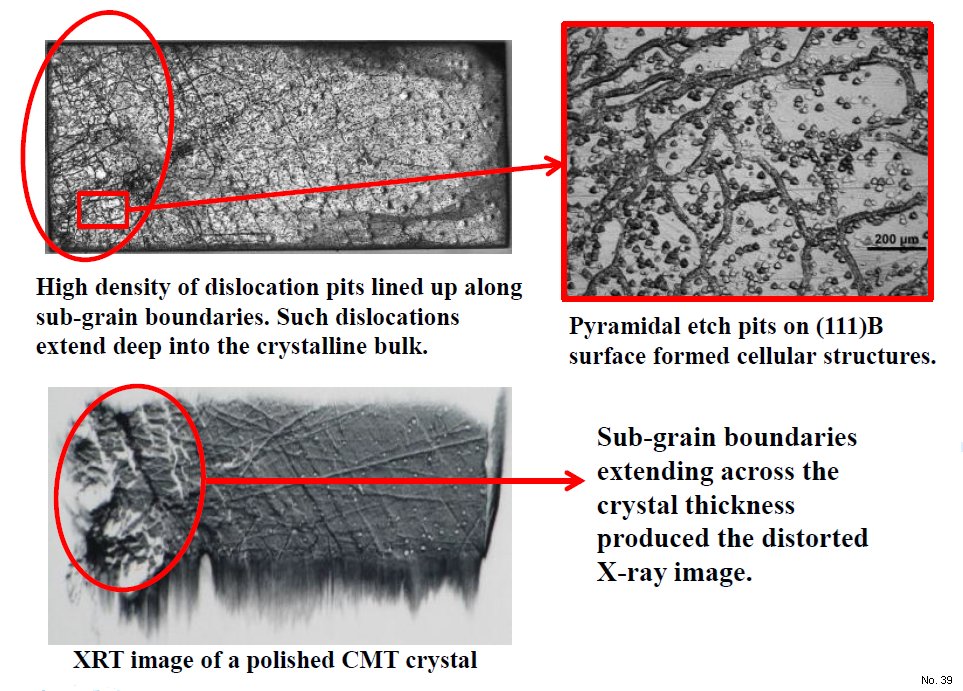
High-Density Dislocation Pits in VB Grown CdMnTe Crystal
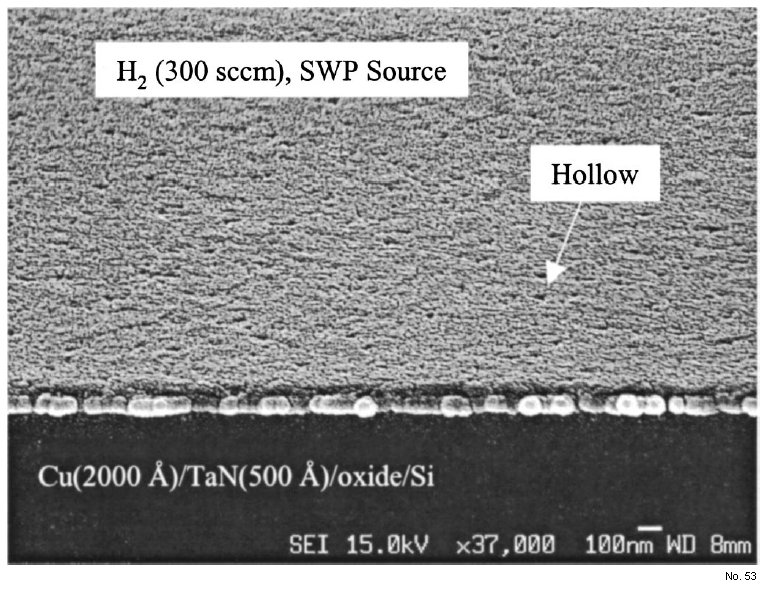
Hollows, Hillocks - Copper Wafer

Humans as Source of Particles I
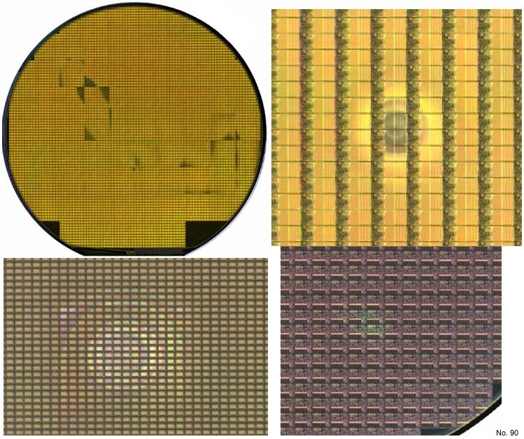
Humans as Source of Particles II

Humans as Source of Particles III
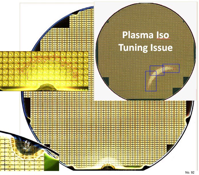
Humans as Source of Particles IV
Humans as Source of Particles V
Humans as Source of Particles VI
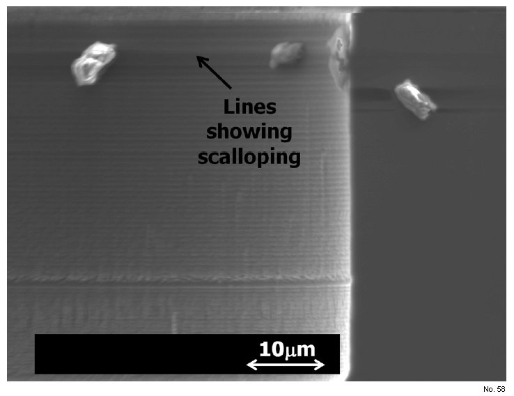
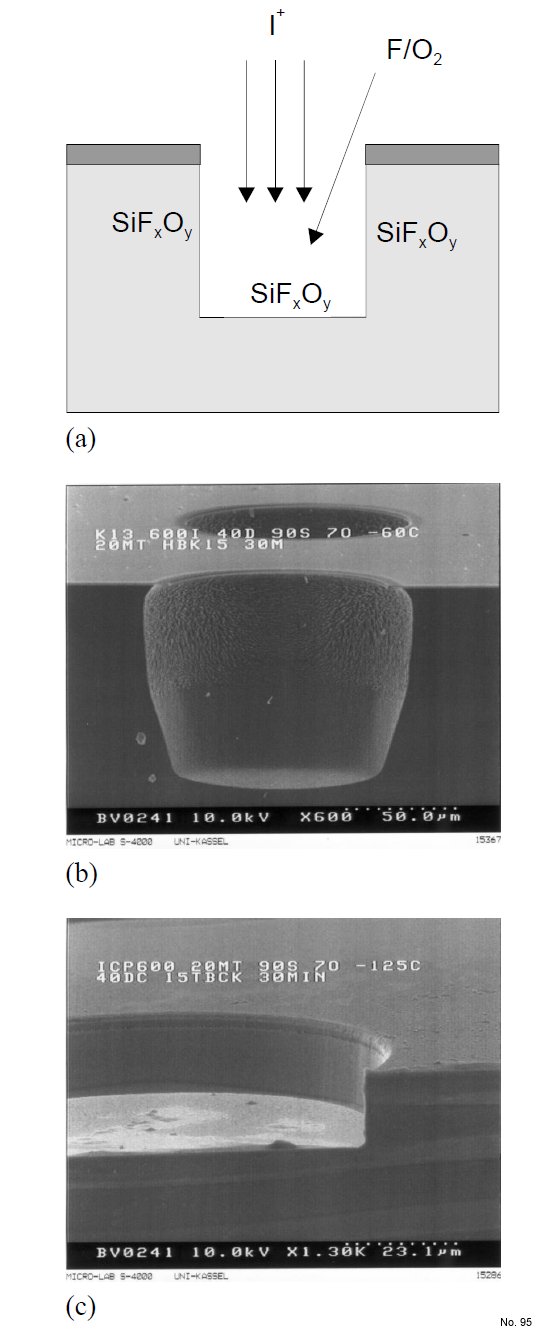
Image Bilayer
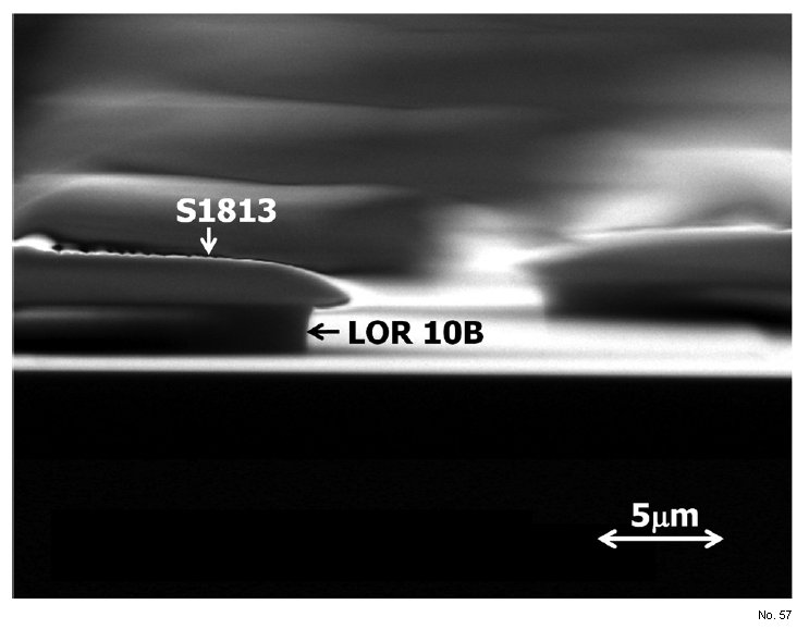
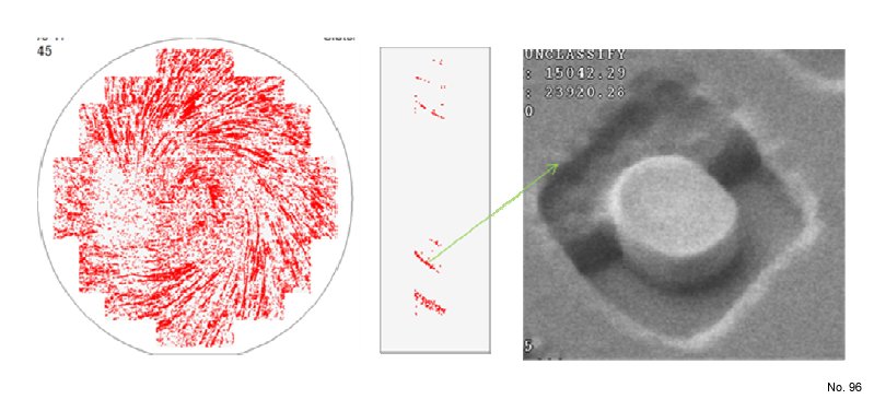
Image Bilayer
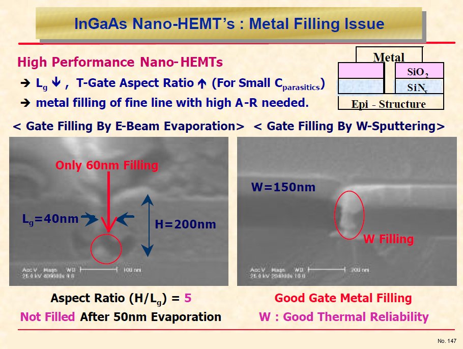
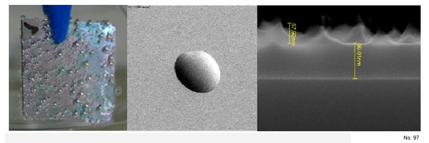
InGaAs Nano-HEMT's Metal Filling Issue
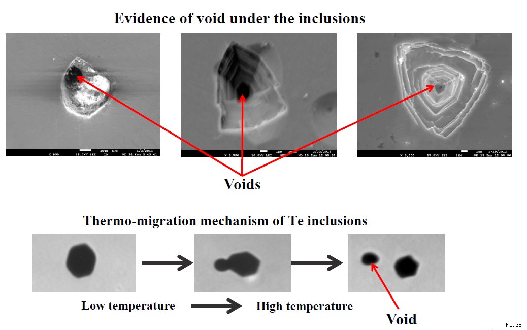
Inclusions with Voids - CdZnTe

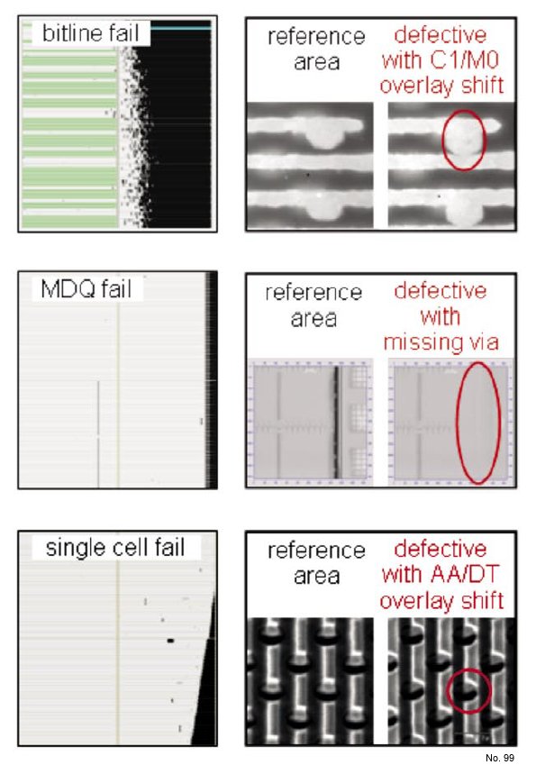
Irregular Wet Etching of Cr Mask
Killer Defect from Aluminum Etch Proces

Killer Defects Generated in Aluminum Metal Etch Processes
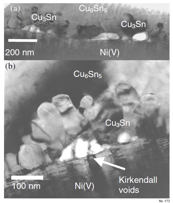
Kirkendall’s Voids
Lens Stepper Macro Defects
Line Corrosion and Scratches
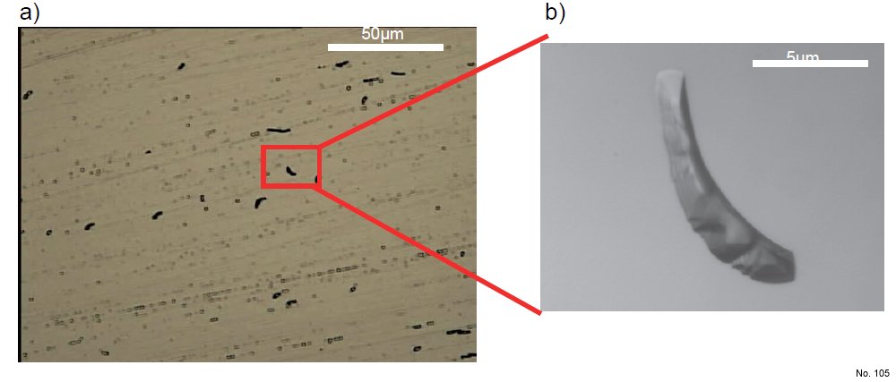
Loading Examples
Low Sample Temperature
Macro-Bubbles and Fiber-Like Inclusions in YCa4O(BO3)3 (YCOB) Crystals
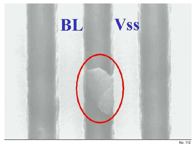
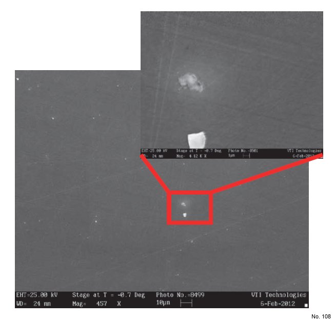
Metal Residue Between BL and VSS-Line I

Metal Residue Between BL and VSS-Line II

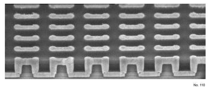
Metal Residue Between BL and VSS-Line III
Metal Residue Between BL and VSS-Line IV
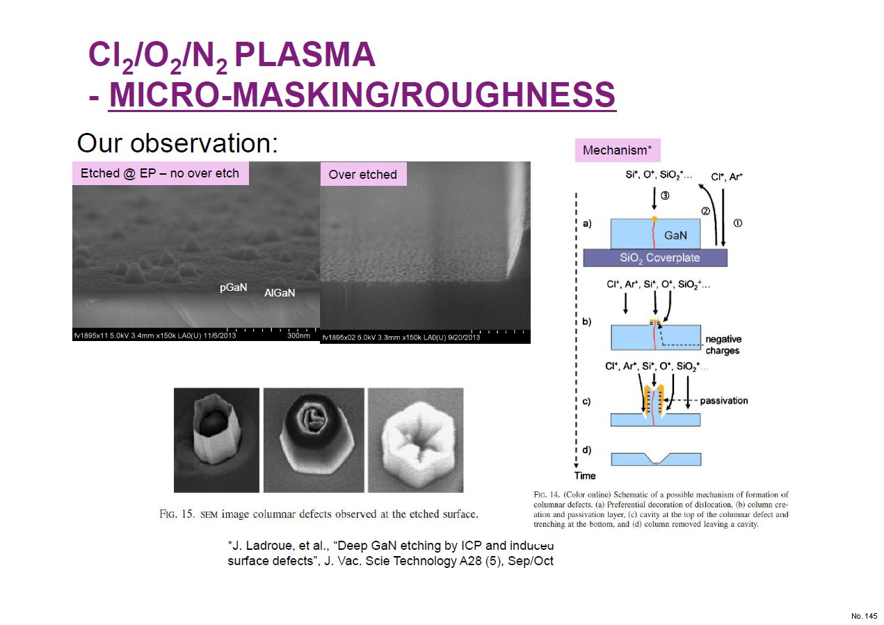
Micro-Masking/Roughness - GaN
Microscope Image of the Surface of Polyimide PI 2611 After Coating
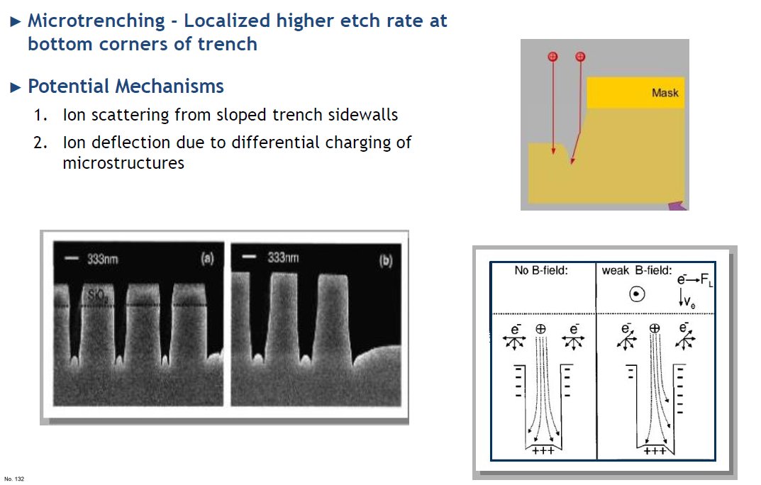
Microtrenching
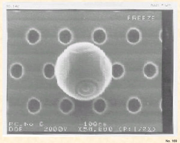
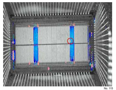
Misaligned Ball
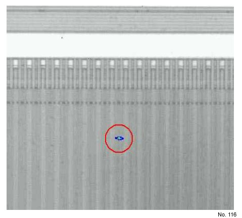
Misalignment
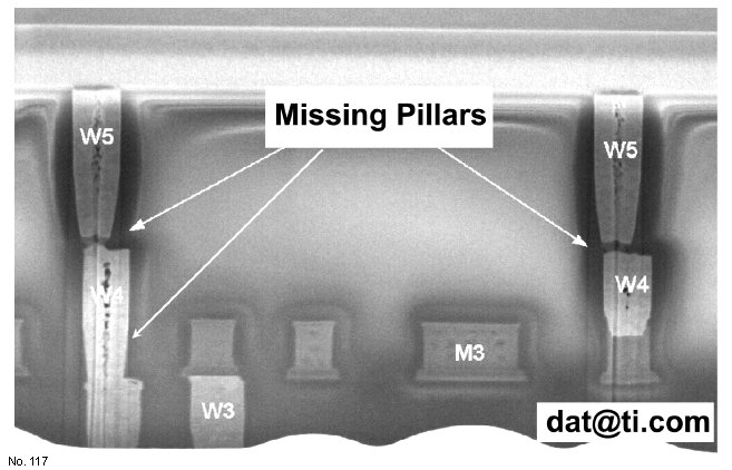
Missing Metal Pillars

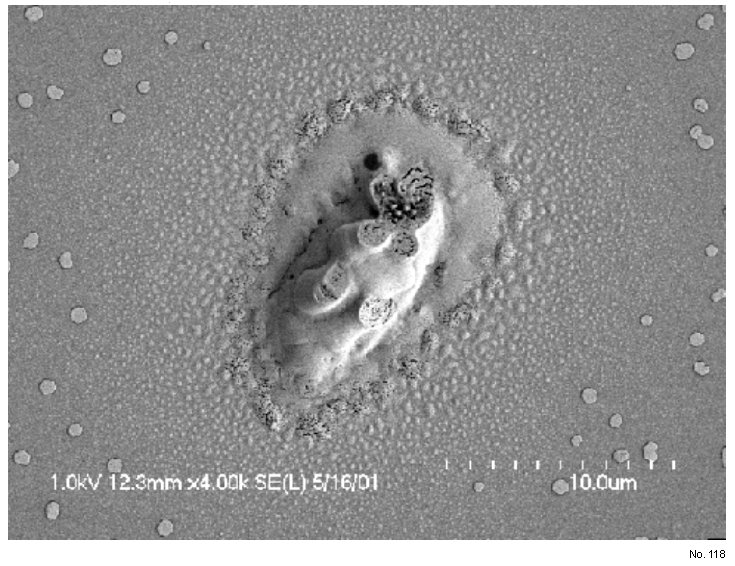
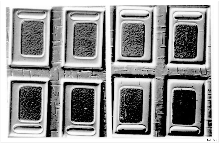
Missing Patterns
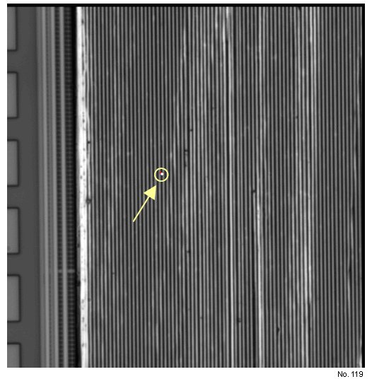
Molten Polysilicon Filaments

Molten Silicon/Aluminum Filament
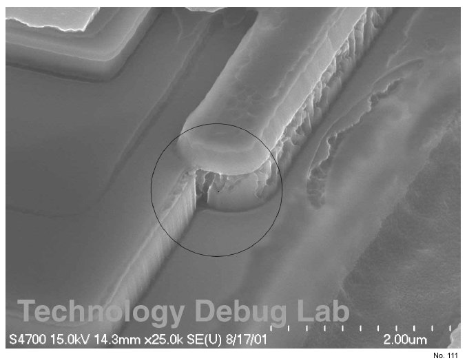
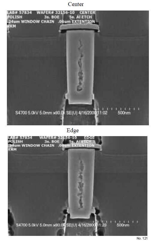
Necking

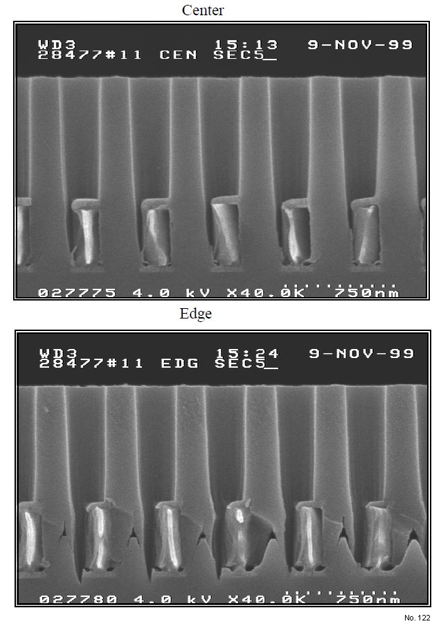
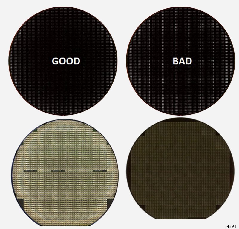
Normal and Bad Etch Results

Open Metal Line

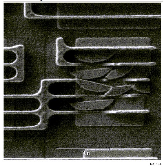
Over Etch - GaN
Over Etch - GaN
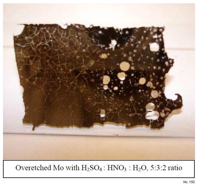
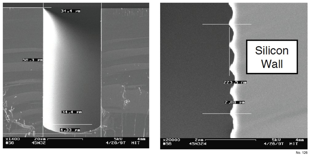
Overetched Mo with H2SO4 HNO3 H2O, 532 Ratio

Overetching of Polyimide Film
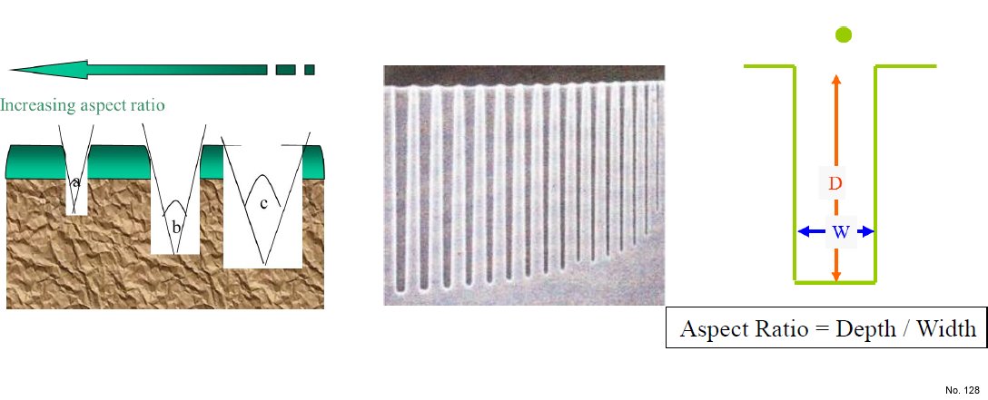
Overlay Shift

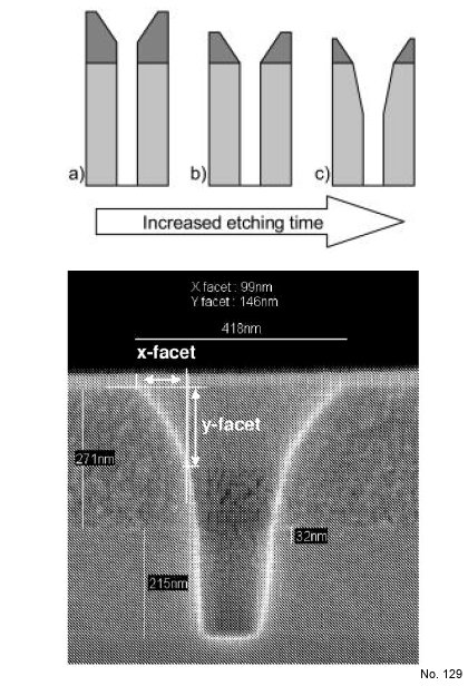
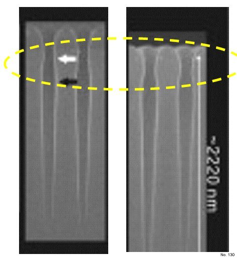
Oxygen Flow Variation - GaN

PVD Coating Peeling
Partial Pattern – No Expose
Particle Defect
Particle Defects
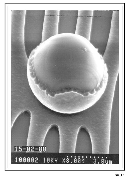
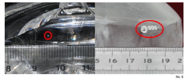
Particles on Chips A Metal Ball
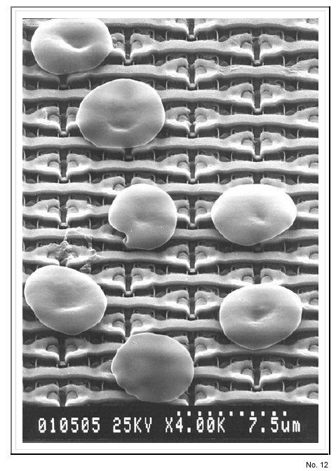
Particles on Chips Blood Cells
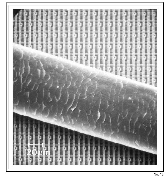
Particles on Chips Hair I
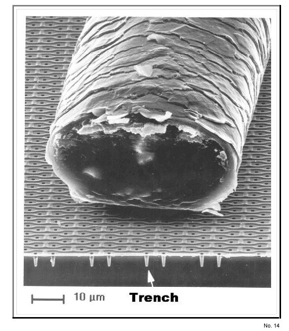
Particles on Chips Hair II
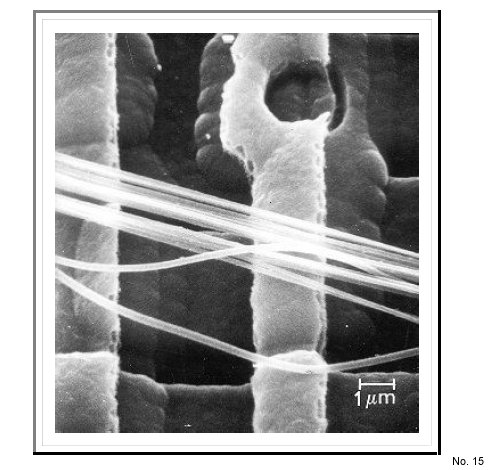
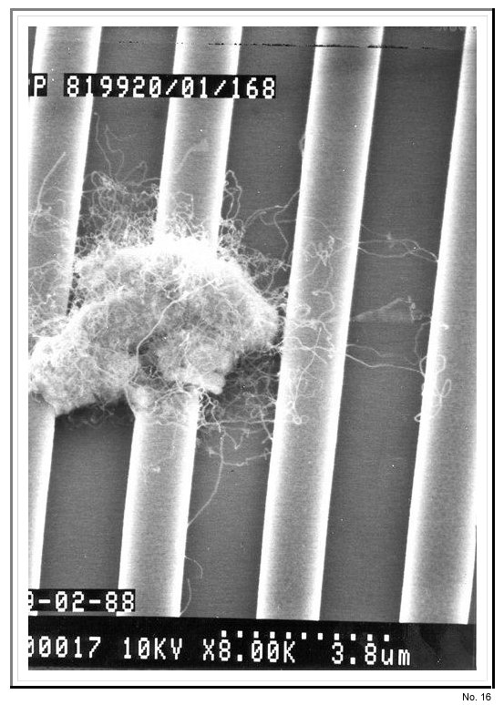
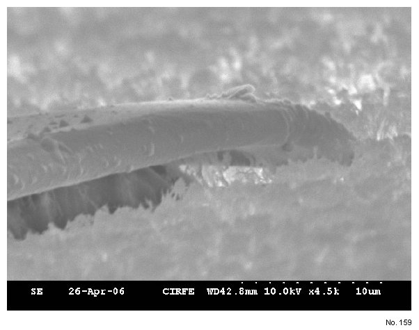
Particles on Chips Spider Silk
Particles on Chips Unknown Object
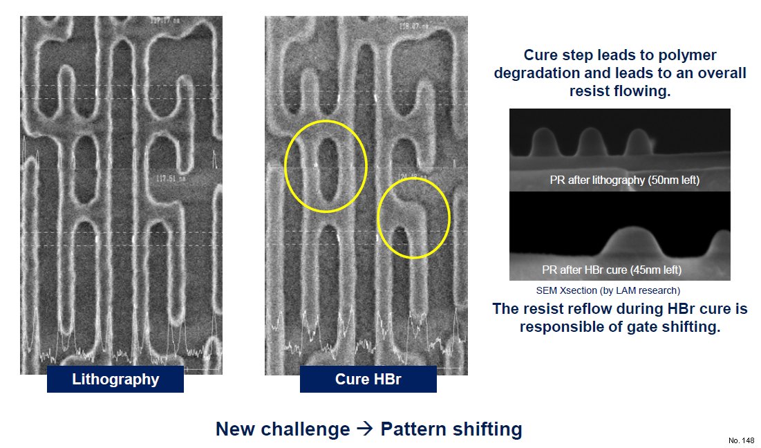
Pattern Shifting - SoC

Photoresist Under-Exposure
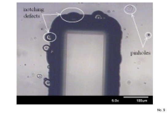
Pinholes Developed in the SiO2
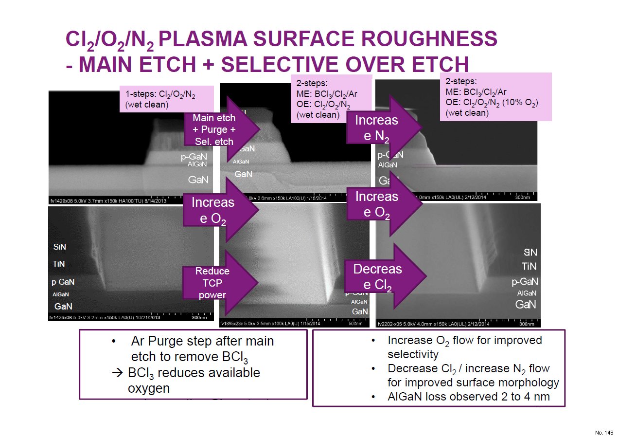
Plasma Surface Roughness - GaN
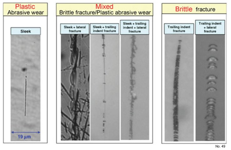
Plastic and Brittle Fracture Scratches
Poly Haze Macro Defect

Poly Short Line

Poly Short Line

Poor Rinse – Macro Defect

Poor Salicide Coverage
Post Metal Etch Residue - Al Layer

Potential Causes of CMP Defects and possible Solutions

Previous Layer Defects
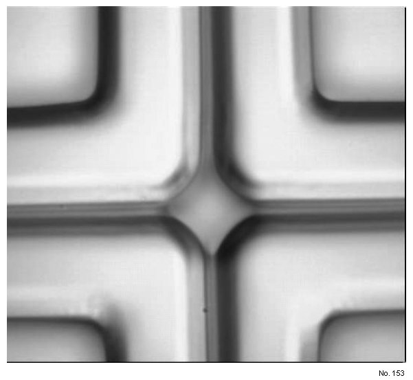
Process Defect
Process Induced Defects in Silicon Wafers
Process Induced Defects Haze
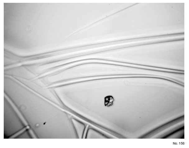
Process Induced Defects Stacking Faults
Pyrex Glass Wafer - Defects Observed on the Etched Glass Surface
RIE Lag

Residue

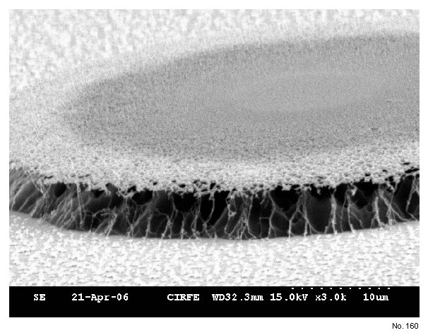
Residue Clinging to Wire Edges
Residue Left from RIE/ICP Etching PI 2611 in O2/CF4

Residue on the Polyimide PI 2611
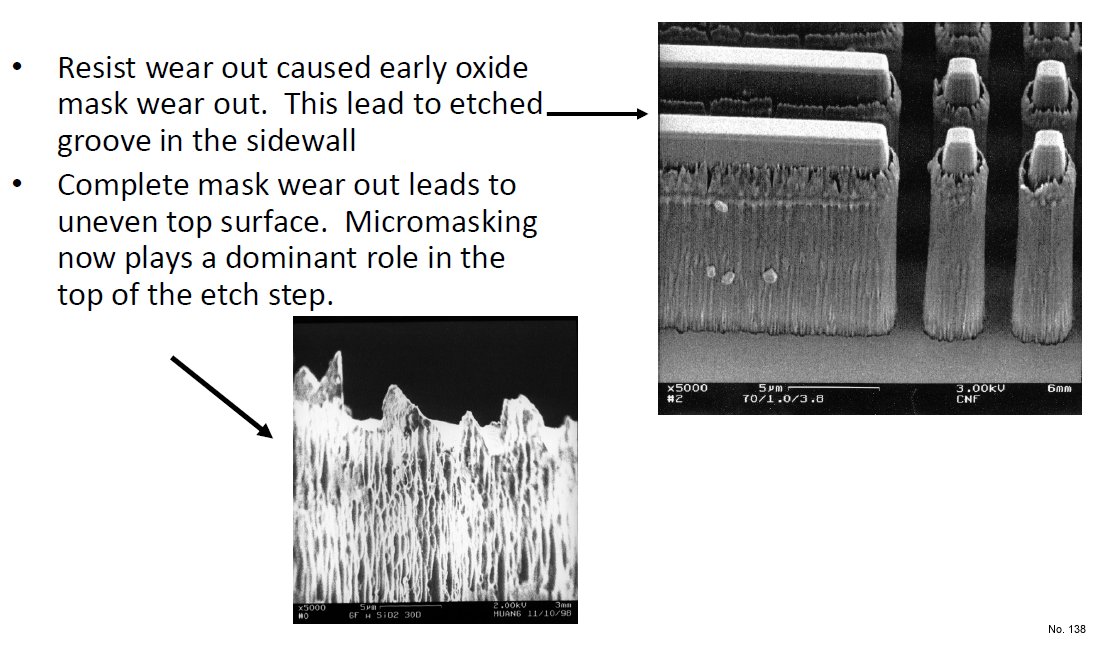
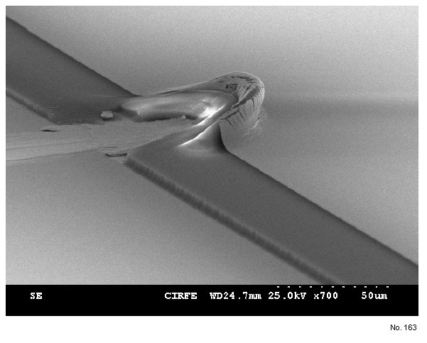
Resist Mask Wear Out
Reticle Tilt Defect
Rework – Scrap Avoidance
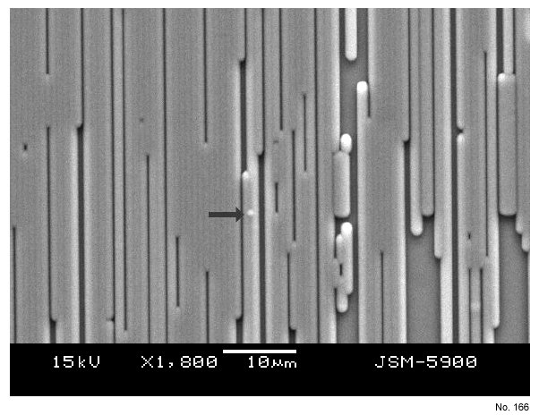
Rework – Yield Improvement
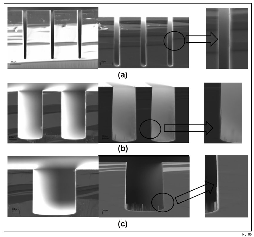
Scalloping - Silicon - Dry etching
Scalloping Effect - Silicon
Scratch Level on STI Patterned Wafers
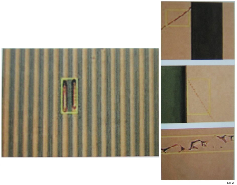
Scratch Through a Polyimide PI 2562 and Cr/Au Film
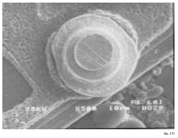
Scratches By Human
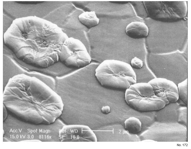
Scratches By Machine

Scratches Formed on STI-Patterned Wafers

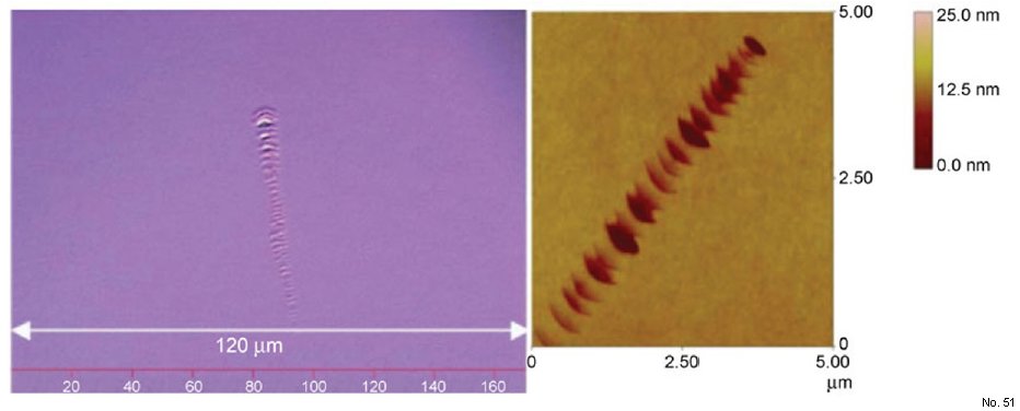
Shallow Etch Pits
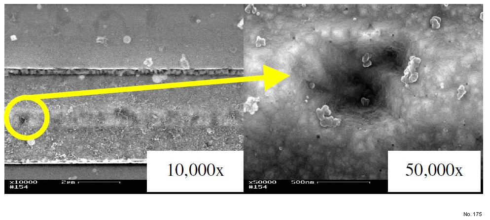
Shallow Grinding Lines
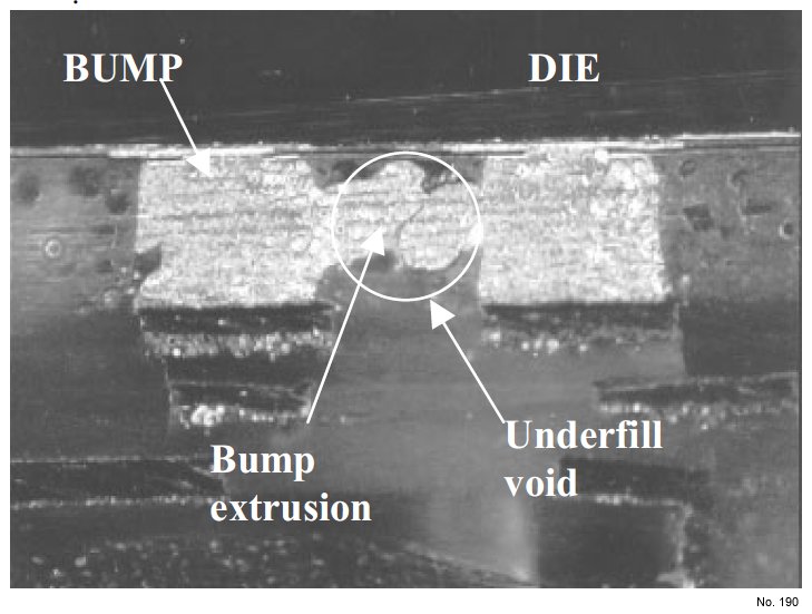
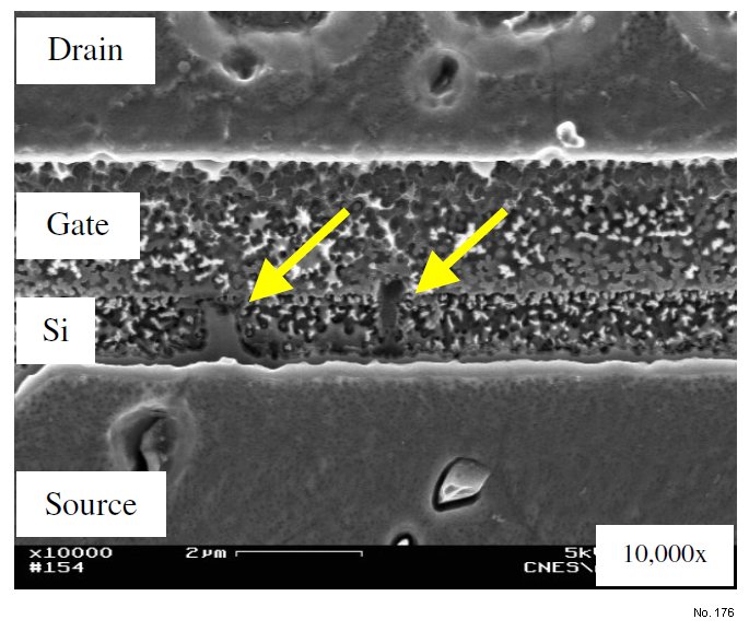
Shorted Bumps
Si Recess Etching Dry Etch
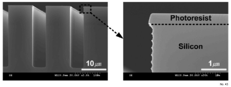
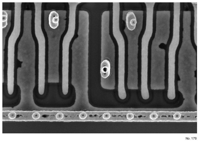
Sidewall Damage - Silicon - Dry Etching
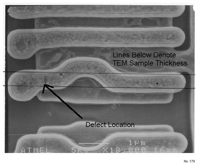
Silicon Defect with Very Gross Electrical Leakage

Size and Density of Star-Shaped Features and Their Effect - CdZnTe

Slanting Edges of Etched Oxide
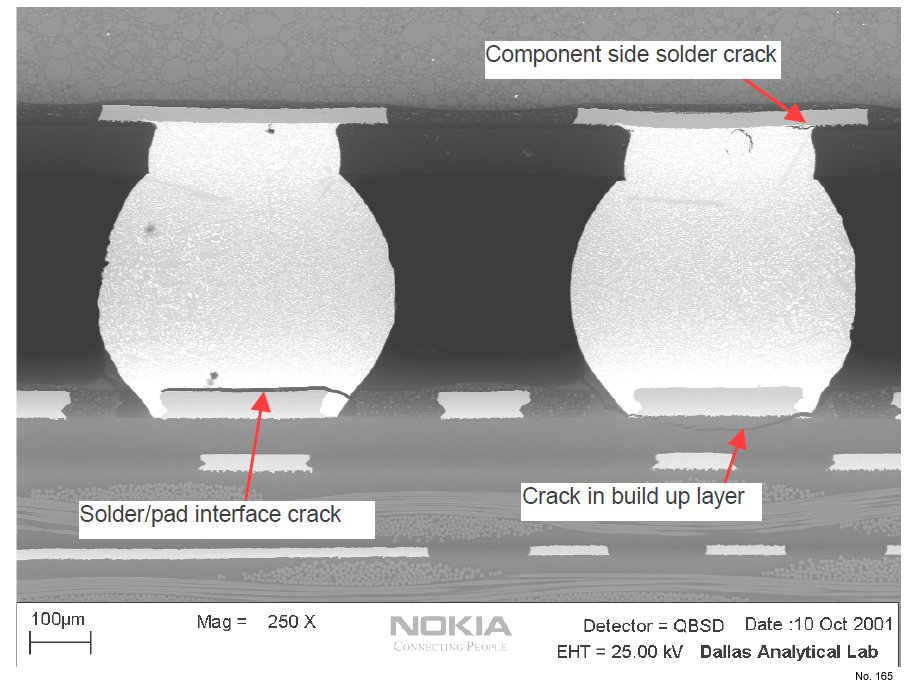
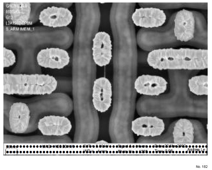
Solder Cracks
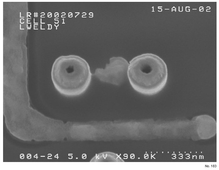
Solder-Bump Short
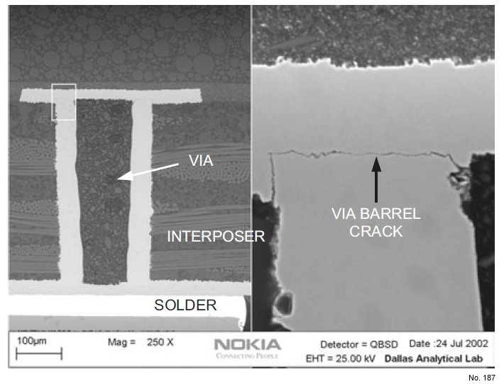
Solder/Pad Interface Crack

Spin Defect on Edge

Spin Defect – Entire Wafer

Spin Defect – Line
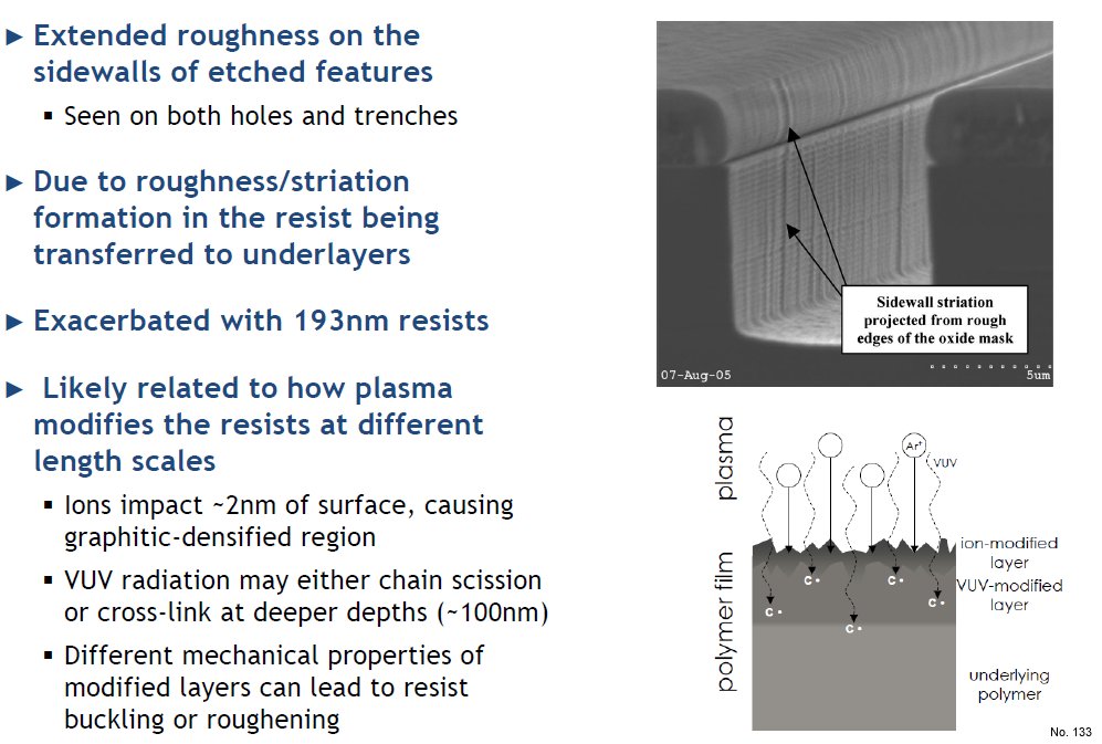
Striations
Sub Surface Cu Voids

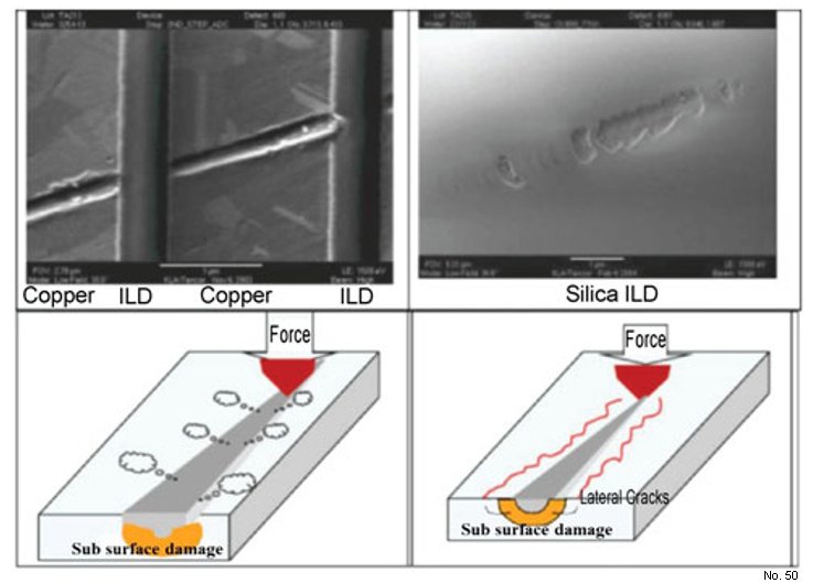
Sub-Surface Damage
Subsurface Damage Caused by Coarse Grinding
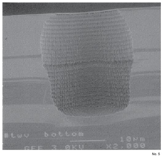
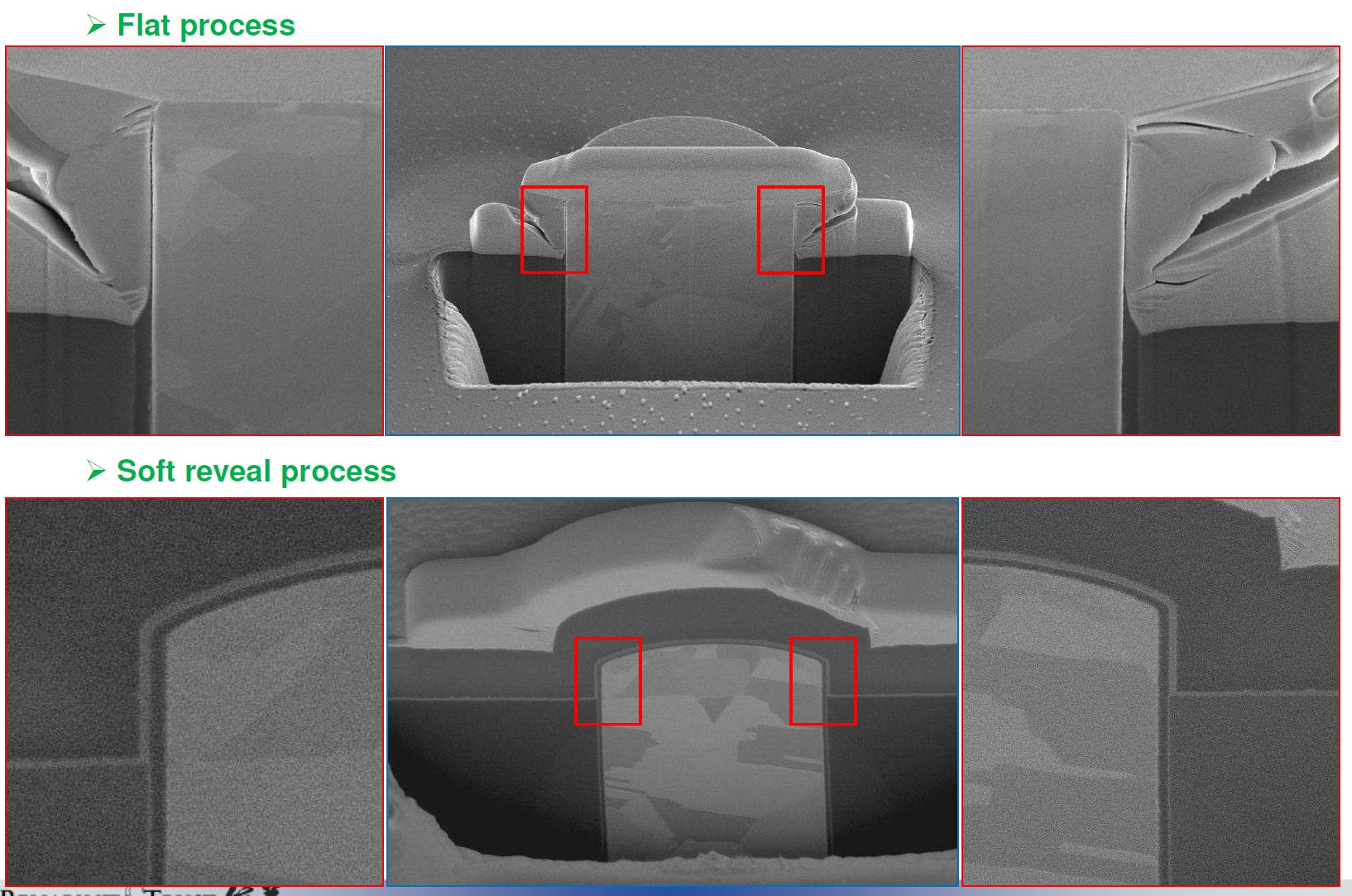
TMDE - Time Multiplexed Deep Etching

The Air We Breath
TiN-Rich Metal Flake Between BL and VSS-Line
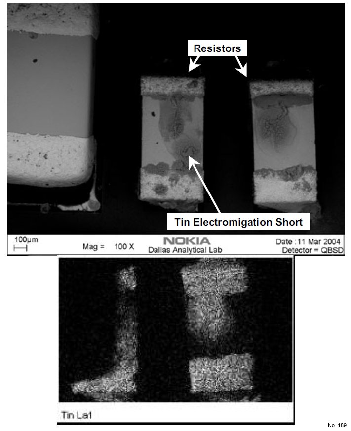
Tin Electrochemical Migration
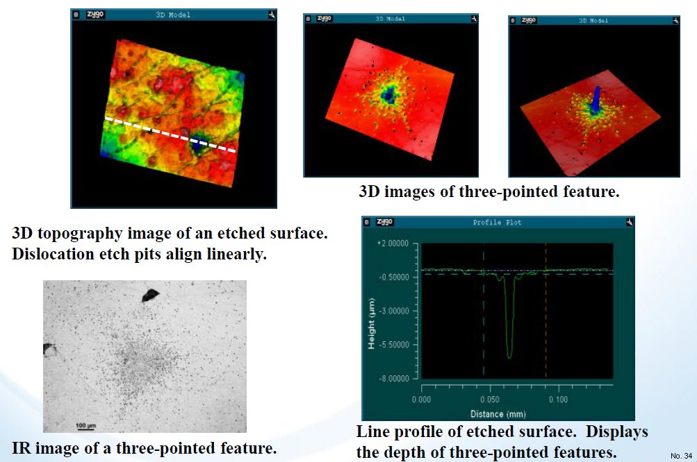
Topographic image of Etched Surface Obtained by Optical Profilometer - CdZnTe
Tornado Shape After Poly-Si Wet Etching
Tungsten (W) Plugs
Tungsten Stringer Between Center Contacts
Tweezer Marks
Underdeveloped Photoresist
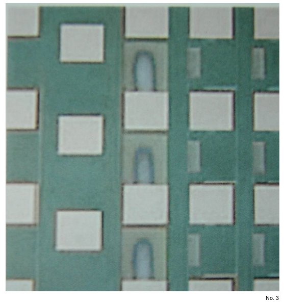
Unfilled Contact

Uniform Etching of PI 2562
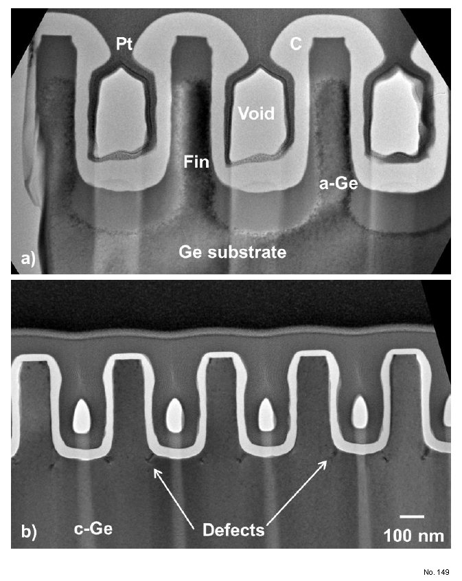
Voids - Germanium
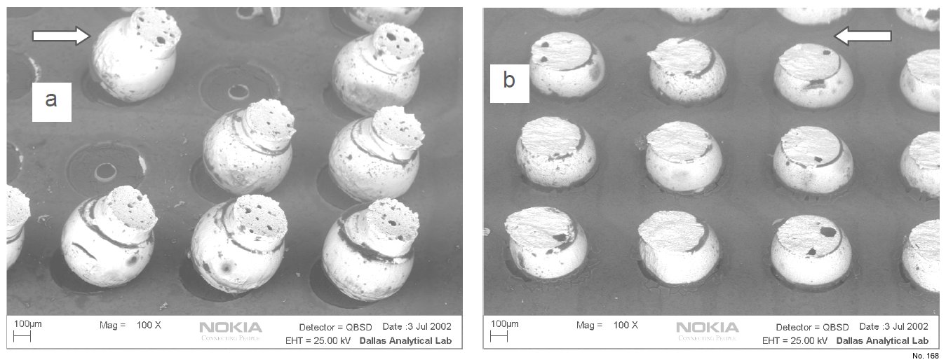
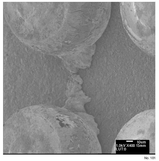
Voids in Solder Ball

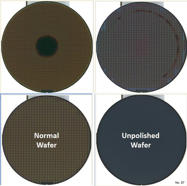
Wafer Contamination – Large
Wafer Contamination – Small
Wafer Edge Discoloration
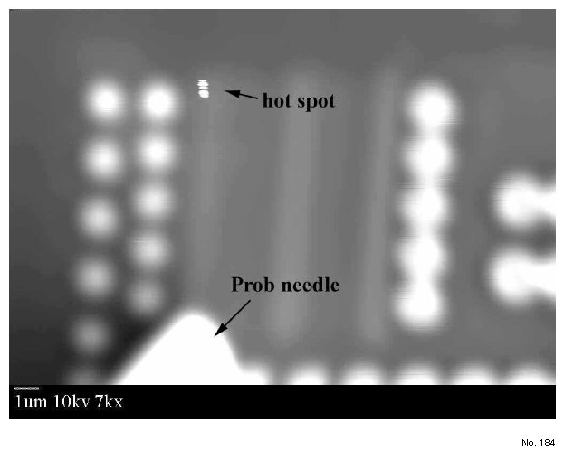
Wafer Hotspot Defects
Wafer Spinning Rate

Water Condensation

XRT and IR Images of Defects in CdZnTe Crystals